External Interfaces
Table of contents:
- USB
- Serial ports
- 1-Wire
- HDMI
- ETHERNET
- GSM
- Wi-Fi/2.4G
- Digital inputs
- Digital inputs/outputs
- Universal inputs/outputs
USB
The device is equipped with 2 USB connectors.
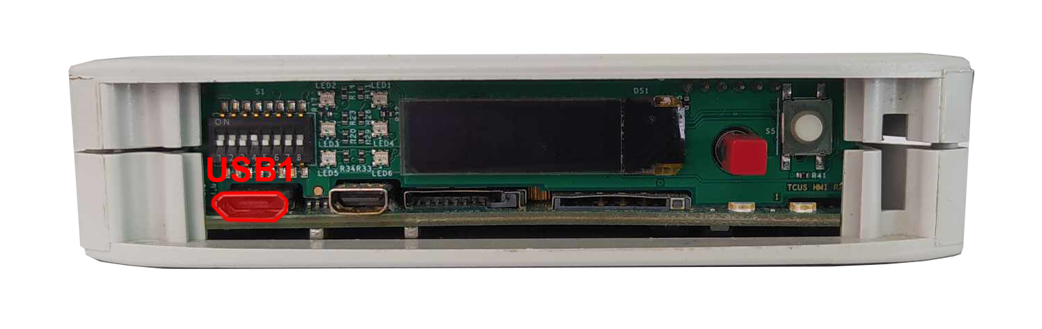
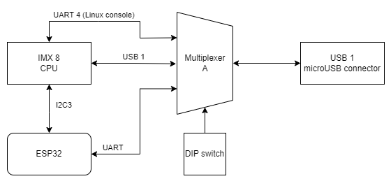
USB1
MicroUSB connector for USB 2.0 is placed on the front panel. The interface can work in both host and device modes. The signal on the connector can be chosen with a switch. Maximum current of the connector is 500 mA.
MicroUSB connector location
USB 1 connection diagram
|
Function |
Processor pin |
Default function |
|---|---|---|
|
5 V USB voltage |
F22 |
USB1_VBUS |
|
USB data differential pair negative |
A22 |
USB1_D_N |
|
USB data differential pair positive |
B22 |
USB1_D_P |
|
USB on the go |
AB10 |
USB1_OTG_PWR |
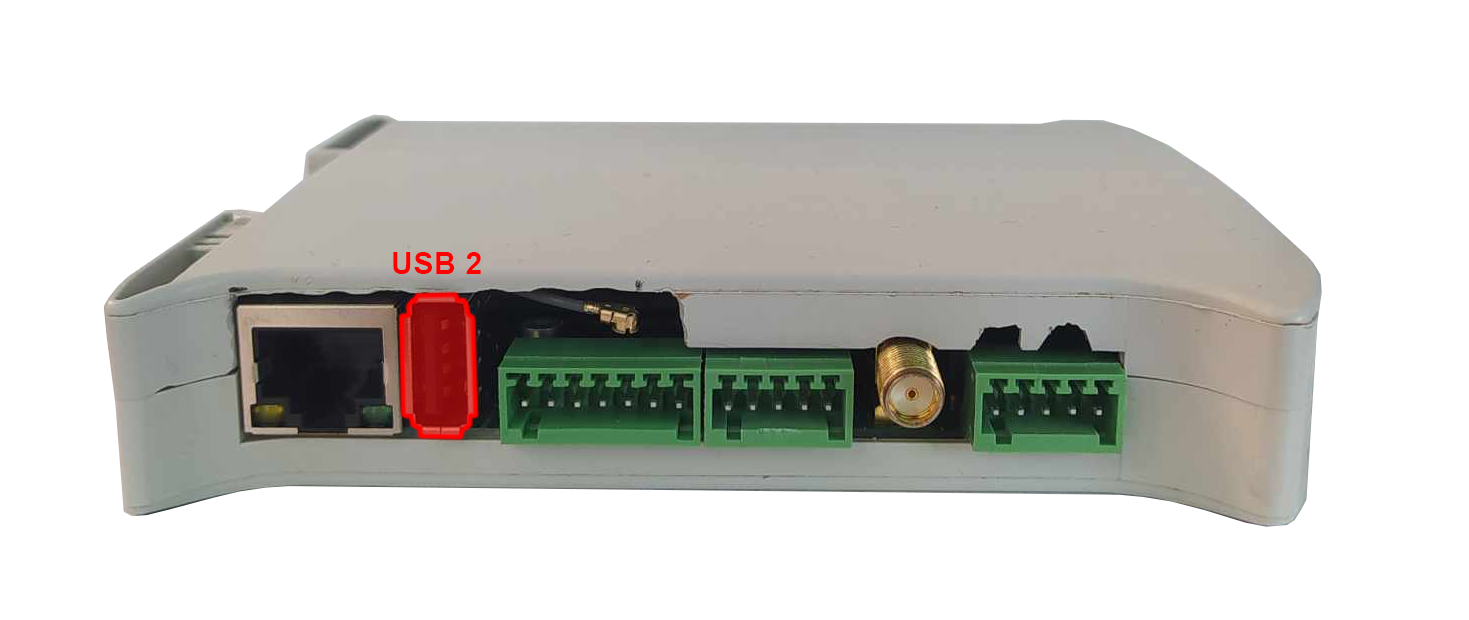
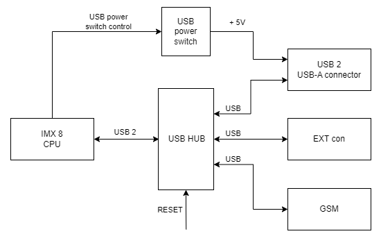
USB2
USB-A connector for USB 2.0 is placed on a side of the device with the interface set up in a host mode. Maximum current of the connector is 1 A.
USB 2 connection diagram
|
Function |
Processor pin |
Default function |
|---|---|---|
|
USB power switch control |
F23 |
USB2_VBUS |
|
USB data differential pair negative |
A23 |
USB2_D_N |
|
USB data differential pair positive |
B23 |
USB2_D_P |
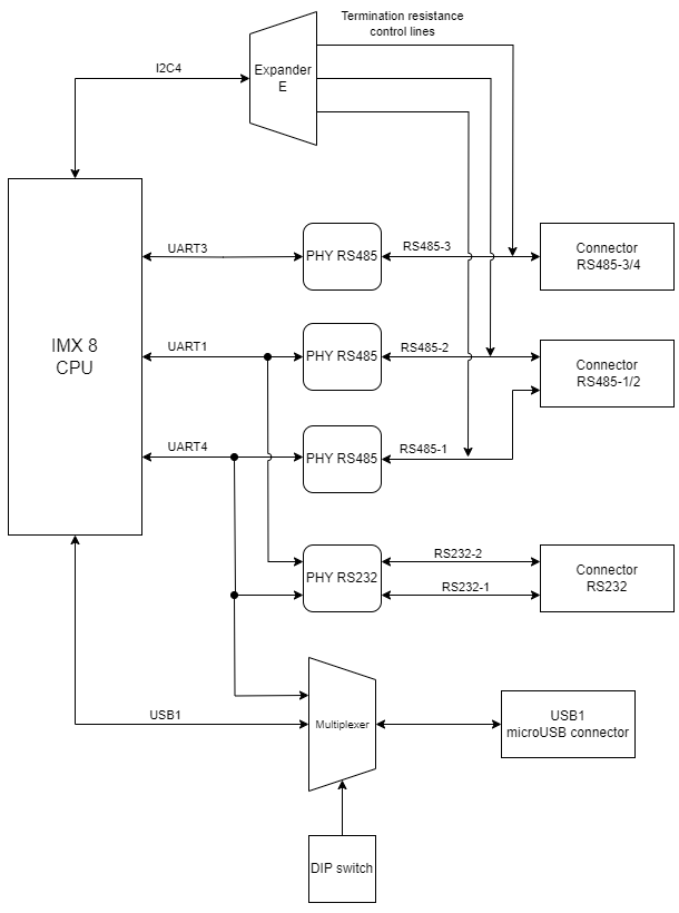
Serial ports
The device is equipped with 3 serial port connectors.
RS485-1/2
Baud rate: 50-115200 bps.
Location of the RS485-1/2 connector
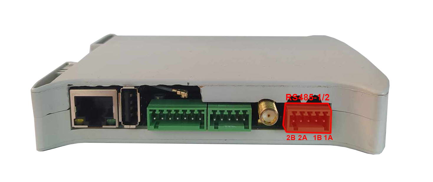
|
Connector pin |
Description |
|---|---|
|
A1 |
RS485 A1 |
|
B1 |
RS485 B1 |
|
G |
Ground |
|
A2 |
RS485 A2 |
|
B2 |
RS485 B2 |
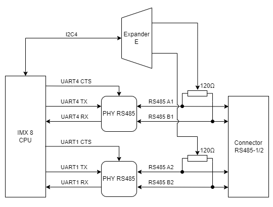
RS485-1/2 connections diagram
UART4
Device name: /dev/ttymxc2
|
Signal |
Processor pin |
Default function |
|
Receive (UART2 RX) |
X |
UART2_RXD |
|
Transmit (UART2 TX) |
X |
UART2_TXD |
UART1
Device name: /dev/ttymxc0
|
Signal |
Processor pin |
Default function |
|
Clock |
D13 |
I2C4_SCL |
|
Data |
E13 |
I2C4_SDA |
RS485-3/4
Baud rate: 50-115200 bps.
Location of the RS485-3/4 connector
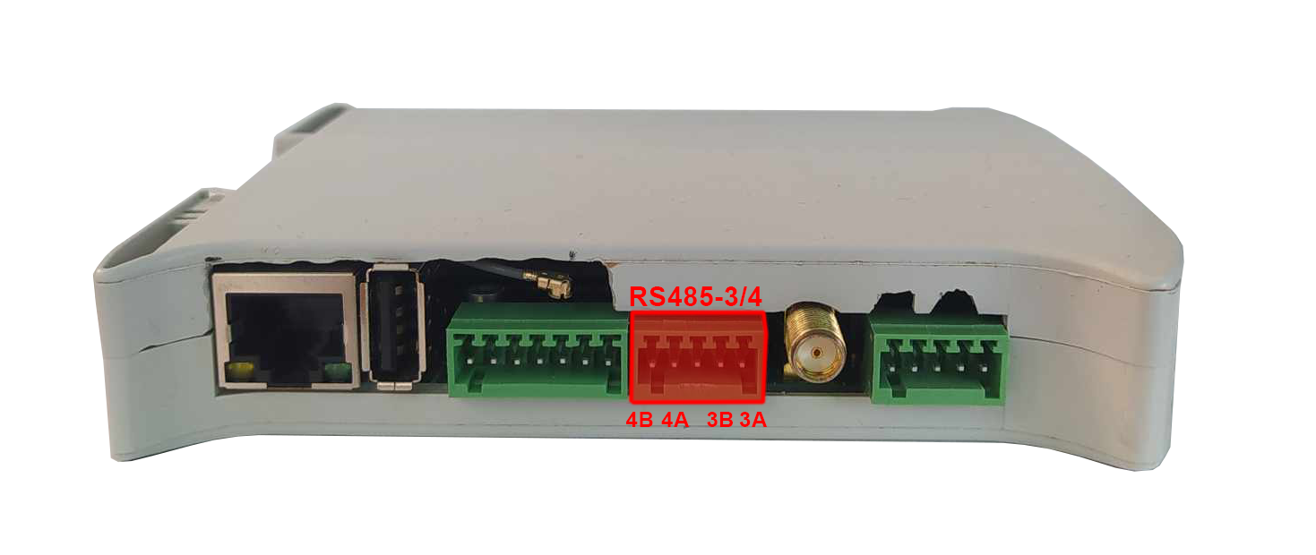
|
Connector pin |
Description |
|---|---|
|
A3 |
RS485 A3 |
|
B3 |
RS485 B3 |
|
G |
Ground |
|
A4 |
RS485 A4 |
|
B4 |
RS485 B4 |
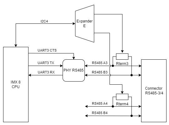
RS485-3/4 connections diagram
UART2
Device name: /dev/ttymxc2
|
Signal |
Processor pin |
Default function |
|
Receive (UART2 RX) |
X |
UART2_RXD |
|
Transmit (UART2 TX) |
X |
UART2_TXD |
RS232-1/2
Baud rate: 50-115200 bps.
Location of the RS232-1/2 connector
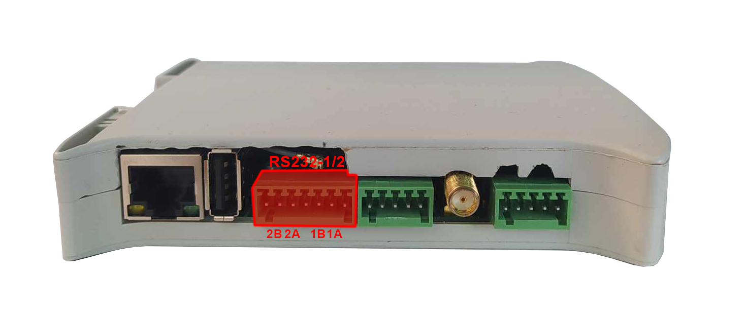
|
Connector pin |
Description |
|---|---|
|
T1 |
RS232 TX1 |
|
R1 |
RS232 RX1 |
|
T2 |
RS232 TX2 |
|
R2 |
RS232 RX2 |
RS232-1/2 connections diagram
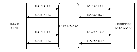
UART4
Device name: /dev/ttymxc2
|
Signal |
Processor pin |
Default function |
|
Receive (UART2 RX) |
X |
UART2_RXD |
|
Transmit (UART2 TX) |
X |
UART2_TXD |
UART1
Device name: /dev/ttymxc0
|
Signal |
Processor pin |
Default function |
|
Clock |
D13 |
I2C4_SCL |
|
Data |
E13 |
I2C4_SDA |
Expander E
The termination resistors are controlled by signals output from the Expander E connected by I2C4 interface with the CPU.
Diagram of serial ports connections
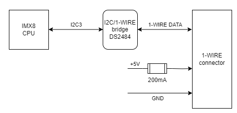
1-Wire
The device is equipped with the 1-Wire interface operating with Maxim sensors. Connector 5 V outputs are secured with a 100 mA fuse.
1-Wire connector and pins
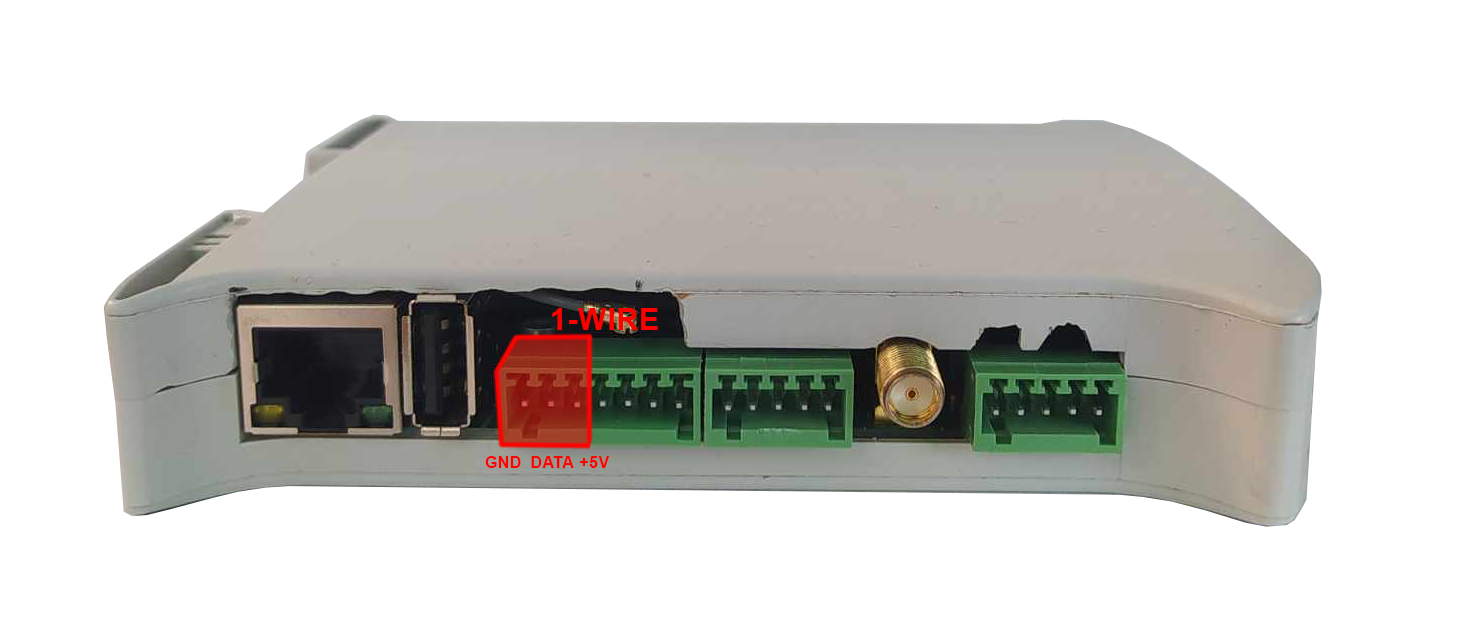
| Connector pin |
Description |
|---|---|
|
1W |
1-Wire data |
|
5V |
1-Wire +5 V power |
|
G |
Ground |
1-Wire connection diagram
I2C2
Device name: /dev/i2c-1
|
Signal |
Processor pin |
Default function |
|
Clock |
D10 |
I2C2_SCL |
|
Data |
D9 |
I2C2_SDA |
1-Wire bridge
Part number: DS2484
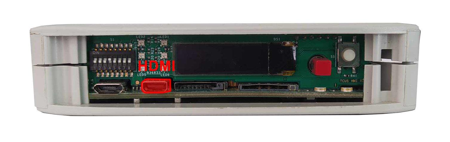
HDMI
The device is equipped with the microHDMI standard connector located on the front panel.
HDMI connector location
|
Signal |
Processor pin |
Default function |
|---|---|---|
|
DSI_TX0_N |
A9 |
MIPI_DSI_TX0_N |
|
DSI_TX0_P |
B9 |
MIPI_DSI_TX0_P |
|
DSI_TX1_N |
A10 |
MIPI_DSI_TX1_N |
|
DSI_TX1_P |
B10 |
MIPI_DSI_TX1_P |
|
DSI_TX2_N |
A12 |
MIPI_DSI_TX2_N |
|
DSI_TX2_P |
B12 |
MIPI_DSI_TX2_P |
|
DSI_TX3_N |
A13 |
MIPI_DSI_TX3_N |
|
DSI_TX3_P |
B13 |
MIPI_DSI_TX3_P |
|
DSI_CLK_N |
A11 |
MIPI_DSI_CLK_N |
|
DSI_CLK_P |
B11 |
MIPI_DSI_CLK_P |
HDMI connection diagram
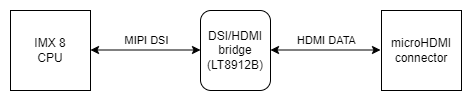
DSI/HDMI Bridge
Part number: LT8912B
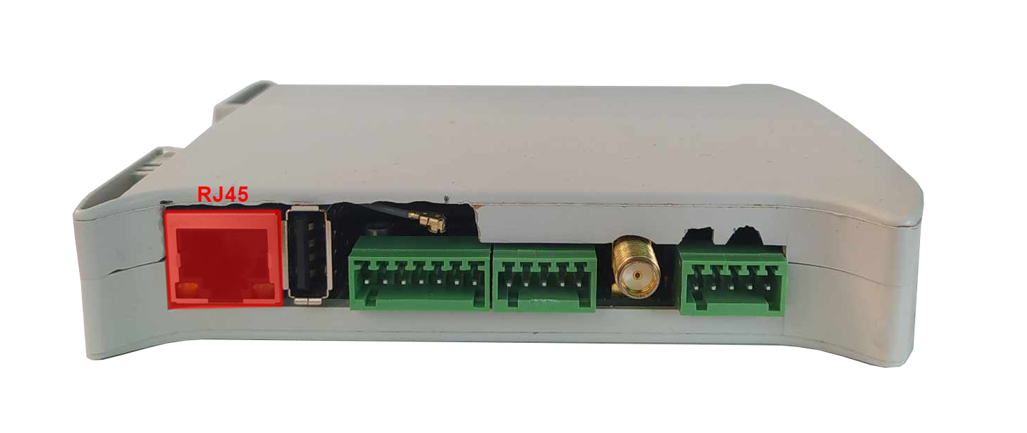
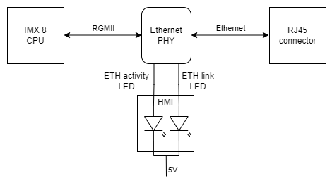
ETHERNET
The device is equipped with a RJ45 connector placed on the side of the device. Diode on the front panel signals ETHERNET's operation.
RJ45 connector location
Ethernet connection diagram
GSM
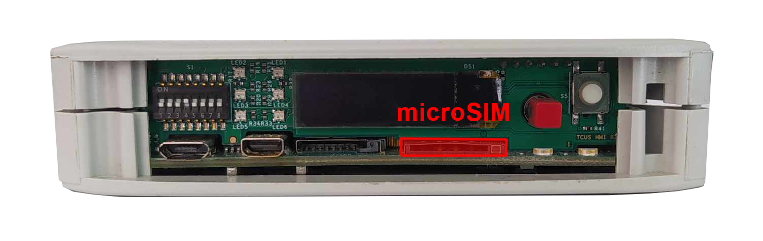
The device is equipped with SIM7600E module connected with miniPCIE connector. Features:
- operation of protocols: CP, UDP, PPP, HTTP, FTP, MQTT, SMS, Mail
- GNSS (GPS, GLONASS, BeiDou) positioning
- microSIM card can be installed
- the device can be expanded with an antenna
- LED diode on the front panel signals GSM operation
MicroSIM connector
|
Function |
Processor pin |
Default function |
|---|---|---|
|
USB power switch control |
F23 |
USB2_VBUS |
|
USB data differential pair negative |
A23 |
USB2_D_N |
|
USB data differential pair positive |
B23 |
USB2_D_P |
GSM connection diagram
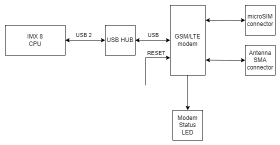
USB HUB
Part number: USB2533
Wi-Fi / Bluetooth
The device is equipped with a Wi-Fi module and can be expanded with a Wi-Fi antenna which takes place of digital inputs no. 1 & 2. The module is dual-band and operates on the frequencies of 2.4 and 5 GHz in 802.11.ac/a/b/g/n standard.
Wi-Fi connections diagram
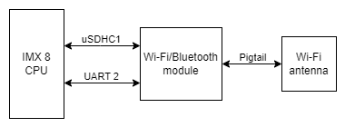
UART 2
Device name: /dev/ttymxc1
Wi-Fi module
Part number: Sterling-LWB5
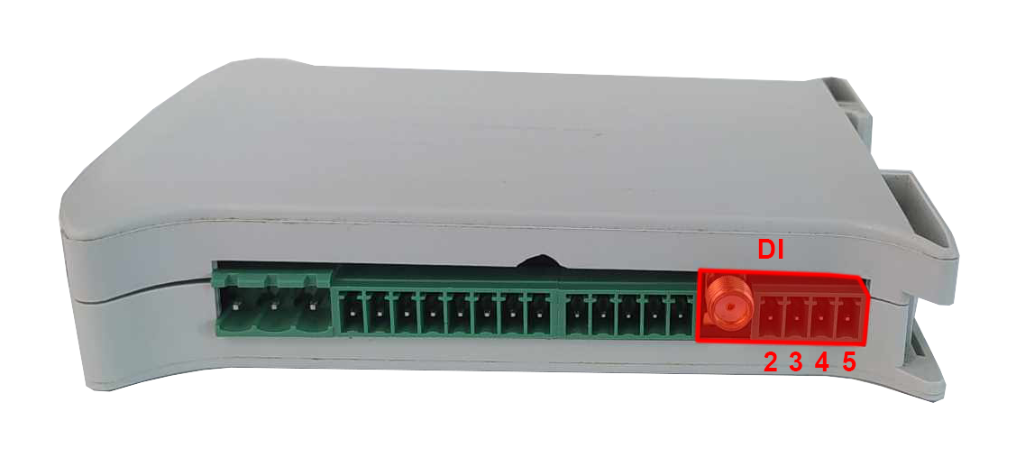
Digital inputs
The device is equipped with a 5 pin digital inputs (DI) connector with a maximum voltage of 30 V and a dry contact. Input signals connect directly to the CPU.
DI location on the connector
|
DO connector pin |
Processor pin |
User space name |
|---|---|---|
|
D1 |
AB15 |
gpiochip2 19 |
|
D2 |
AD18 |
gpiochip2 21 |
|
D3 |
AD13 |
gpiochip2 23 |
|
D4 |
AC14 |
gpiochip2 22 |
|
D5 |
AC15 |
gpiochip2 20 |
DI circuit block schematic
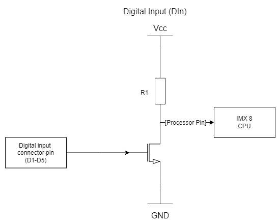
Where:
- R1 - pushup resistor
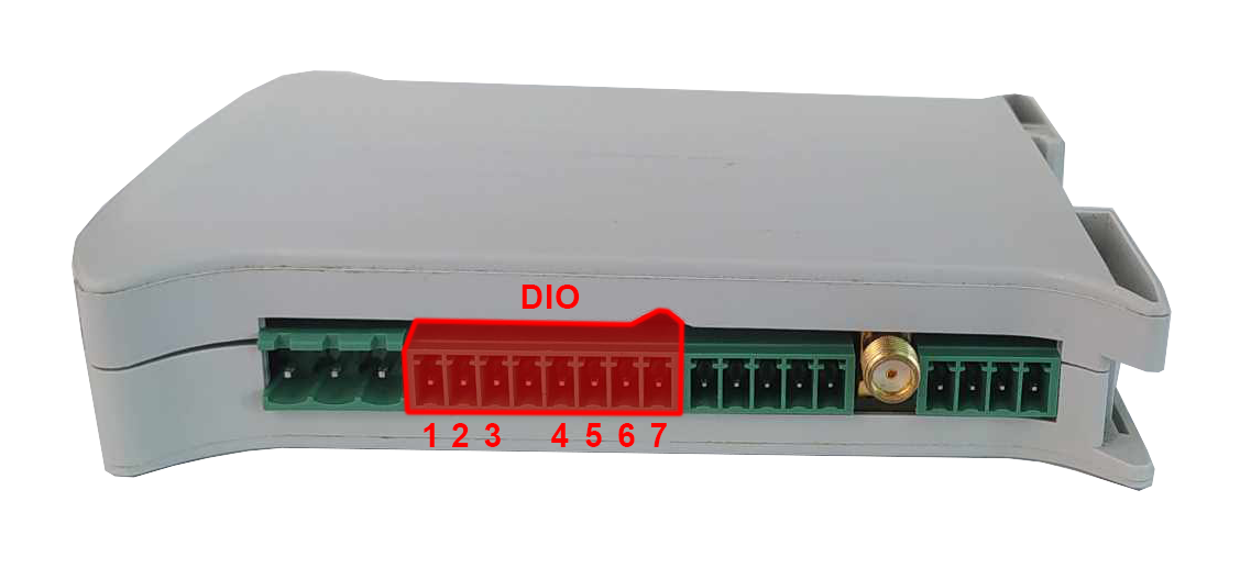
Digital inputs/outputs
The device is equipped with 7 digital input/output (DIO) connectors. They can operate as:
- binary input with a maximum voltage 30 V and a dry contact
- binary Vin output with maximum current 200 mA
DIO location on the connector
|
DIO connector pin |
Input |
Output |
||
|---|---|---|---|---|
|
User space name |
Expander E pin |
User space name |
Expander A pin |
|
|
H1 |
gpiochip5 9 |
26 |
gpiochip8 1 |
1 |
|
H2 |
gpiochip5 10 |
27 |
gpiochip8 2 |
2 |
|
H3 |
gpiochip5 11 |
28 |
gpiochip8 3 |
3 |
|
H4 |
gpiochip5 12 |
1 |
gpiochip8 4 |
4 |
|
H5 |
gpiochip5 13 |
2 |
gpiochip8 5 |
5 |
|
H6 |
gpiochip5 14 |
3 |
gpiochip8 6 |
6 |
|
H7 |
gpiochip5 15 |
4 |
gpiochip8 7 |
7 |
DIO circuit block schematic
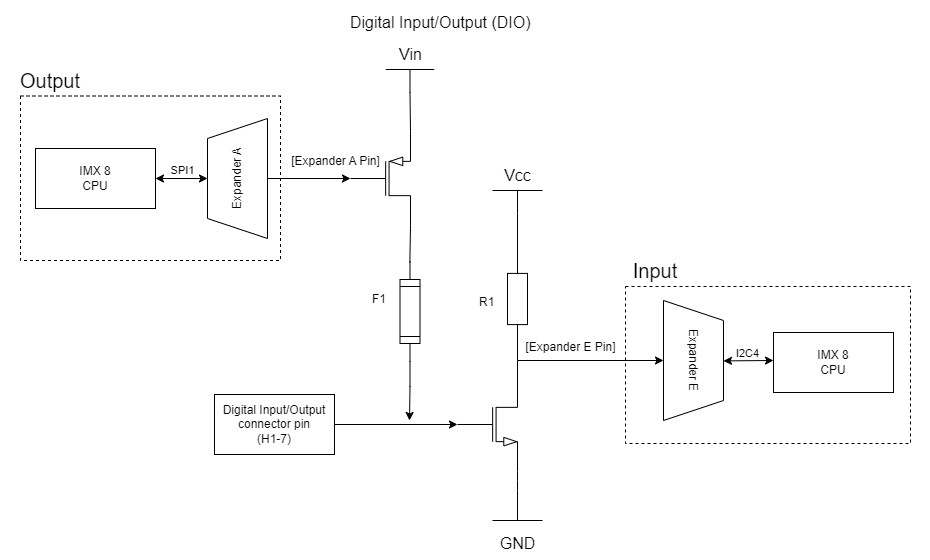
Where:
- F1 - 200 mA fuse
- R1 - pullup resistor 4k7 Ω
Expander E
Inputs of the circuit are connected to the expander E via I2C4 interface.
Expander A
Outputs of the circuit are connected to the expander A via SPI1 interface.
Universal inputs/outputs
The device is equipped with 4 universal analog-digital inputs/outputs (UIO). They can operate as:
- DC voltage inputs for voltage in range of 0-10 V with input resistance of 100 kΩ
- current inputs for current in range of 0-4-20 mA with input resistance of 200 Ω
- current outputs with range of 4-20 mA
- temperature inputs of sensors: Pt1000, Ni1000, KTY, NTC
- resistance inputs with range of 0-5000 Ω
- dry contact inputs
- analog to digital converters with 24-bit resolution
- digital to analog converters with 12-bit resolution
Voltage is measured using a two channel analog to digital converter with 24-bit resolution.
Current value can be set using a 4-channel digital to analog converter.
UIO location on the connector
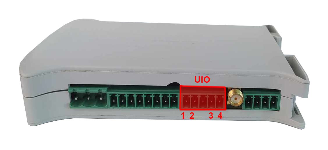
Diagram of UIO circuit
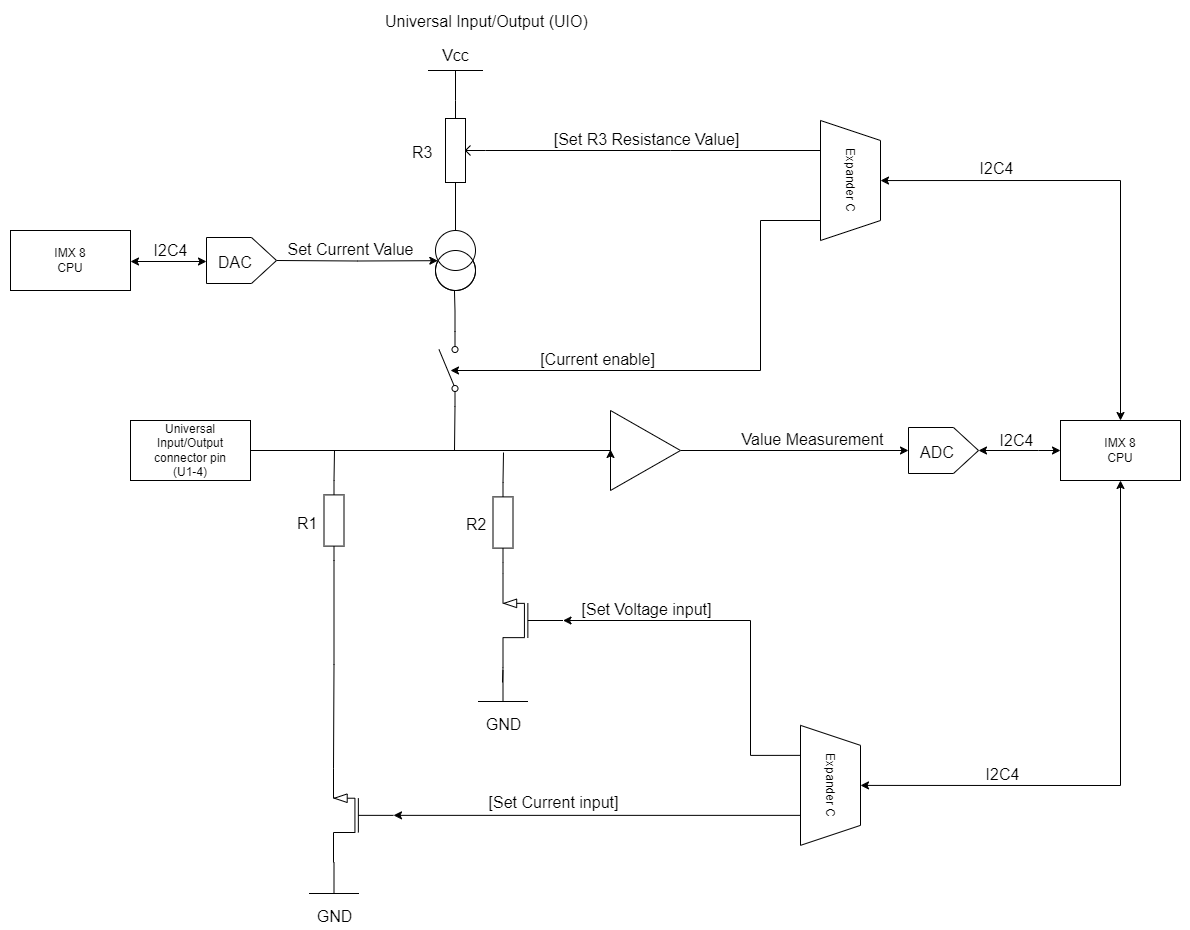
Where:
- R1 - 200 Ω/1% measurement resistor
- R2 - 100 kΩ/1% measurement resistor
- R3 - changeable resistor for changing range of current sources; it can be: 649 Ω/1% or 1,649 Ω/1%
User space access
Analog-Digital Converter A Device name: /sys/bus/iio/devices/iio:device0
Analog-Digital Converter B Device name: /sys/bus/iio/devices/iio:device1
Digital-Analog Converter A Device name: /sys/bus/iio/devices/iio:device2
Possible configurations
Switching to particular modes of the circuit is realized by “Set Voltage Input”, “Set Current Input”, “Current Enable”, “Set R3 Resistance Value” and “Set Current Value” signals.
|
Configuration signal |
Modes of operation |
|||
|---|---|---|---|---|
|
DI dry contact |
AI 0-10 V |
AI 0-4-20 mA |
AO 4-20mA / temperature* / resistance |
|
|
Set Voltage Input |
0 |
1 |
0 |
0 |
|
Set Current Input |
0 |
1 |
0 |
1 |
|
Current Enable |
1 |
0 |
0 |
1 |
|
Set R3 Resistance value |
1 |
X |
X |
1 or 0** |
|
Set Current Value |
12-bit value*** |
X |
X |
12-bit value*** |
* by measuring resistance
** 1 for 1,649 kΩ/1% or 0 for 649 Ω/1% resistor
*** depends on the sensor (see examples for more)
Where:
- X - any value
- DI - digital input
- AI - analog input
- AO - analog output
|
UIO connector pin |
Configuration signal |
Expander pin |
|---|---|---|
|
U1 |
Current enable |
20 |
|
Set voltage input |
19 |
|
|
Set current input |
27 |
|
|
Set R3 resistance value |
21 |
|
|
U2 |
Current enable |
3 |
|
Set voltage input |
22 |
|
|
Set current input |
28 |
|
|
Set R3 resistance value |
4 |
|
|
U3 |
Current enable |
23 |
|
Set voltage input |
17 |
|
|
Set current input |
1 |
|
|
Set R3 resistance value |
18 |
|
|
U4 |
Current enable |
26 |
|
Set voltage input |
24 |
|
|
Set current input |
2 |
|
|
Set R3 resistance value |
25 |
Expander C
Inputs of the circuit are connected to the expander C via I2C4 interface.