Hardware
- Introduction
- Technical Diagrams
- External Interfaces
- Internal Devices
- Front Panel
- Expanders
- Connectors Designations
Introduction
Tiger City IMX Industrial Computer with Linux OS
The Tiger City IMX minicomputer uses Linux operating systems and is equipped with several communication interfaces such as: Ethernet, USB 2.0, HDMI, GSM, RS232, RS485, 1-Wire and multiple analog-digital inputs and outputs. It can also be configured to include a Wi-Fi module and encryption modules that increase the security of the device. The casing enables installation on the DIN rail. The front panel has switches, an OLED display and a joystick for manual control of the device operation.
Specifications of the device
- Power: voltage 12-24 VDC +-20%, maximum power 25 W, reverse polarity protection
- SoM: VAR-SOM-MX8M-MINI
- Core: NXP’s i.MX 8M Mini with 1.6 GHz Quad-core ARM Cortex-A53 and 400 MHz Cortex-M4 real-time processor
- Timing: 1.6 GHz
- RAM: 2 GB DDR4
- Flash eMMC: 16 GB
- 1x microSD connector
- 1x microHDMI 1.3a (optional)
- 1x microUSB 2.0 HOST / OTG, max. 500 mA (optional)
- 1x USB-A 2.0 HOST, max. 1 A
- 1x modem GSM SIM7600E + microSIM (optional)
- 1x 1-Wire (optional)
- 7x DIO - digital input/output, max. 30 V
- 4x UIO - universal analog-digital input/output (temperature measurement with sensors, e.g.: Pt1000, Ni1000, KTY, NTC, current, voltage and resistance sensors), max. 20 V (optional)
- 5x DI - digital input (3 x DI), max. 30 V (optional)
- 2x RS232, baudrate 50-115200 bps
- 2x RS485, baudrate 50-115200 bps (4x optional)
- 1x Ethernet 10/100 Mbps - RJ45 connector
- 1x Wi-Fi® / 2.4G module (optional)
- 1x secure element (optional)
- 1x display OLED 0.87" 128x32 px black&white (optional)
- 1x Joystick (optional)
- RTC (optional), buzzer, EEPROM
- TPM (optional)
- Software watchdog
Dimensions of the device
The space that the device occupies can be approximated to a cube of the following dimensions: 119 mm x 101 mm x 22.5 mm.
Simplified block diagram

Technical Diagrams
Tiger City IMX Industrial Computer with Linux OS
Enclosure
Placement of peripherals

Detailed connections diagram

External Interfaces
Tiger City IMX Industrial Computer with Linux OS
- USB
- Serial ports
- 1-Wire
- HDMI
- ETHERNET
- GSM
- MicroSD slot
- Wi-Fi/2.4G
- Digital inputs
- Digital inputs/outputs
- Universal inputs/outputs
USB
The device is equipped with 2 USB connectors.
USB1
MicroUSB connector for USB 2.0 is placed on the front panel. The interface can work in both host and device modes. The signal on the connector can be changed with a switch. The maximal current of the connector is 500 mA.
MicroUSB connector location

USB1 connection diagram

|
Description |
Processor pin |
Default function |
|
5 V USB voltage |
F22 |
USB1_VBUS |
|
USB data differential pair negative |
A22 |
USB1_D_N |
|
USB data differential pair positive |
B22 |
USB1_D_P |
|
USB on the go |
AB10 |
USB1_OTG_PWR |
UART4
Device name: /dev/ttymxc3
|
Signal |
Processor pin |
Default function |
|
Receive (UART4 RX) |
F19 |
UART4_RXD |
|
Transmit (UART4 TX) |
F18 |
UART4_TXD |
USB2
USB-A connector for USB 2.0 is placed on the side of the device with the interface set up in the host mode. The maximal current of the connector is 1 A.
USB-A connector location
USB2 connection diagram

| Description |
Processor pin |
Default function |
|
USB power switch control |
F23 |
USB2_VBUS |
|
USB data differential pair negative |
A23 |
USB2_D_N |
|
USB data differential pair positive |
B23 |
USB2_D_P |
Serial ports
The device is equipped with 3 serial port connectors.
RS485-1/2
Baud rate: 50-115200 bps.
Location of the RS485-1/2 connector
|
Connector pin |
Description |
|
A1 |
RS485 A1 |
|
B1 |
RS485 B1 |
|
G |
Ground |
|
A2 |
RS485 A2 |
|
B2 |
RS485 B2 |
RS485-3/4
Baud rate: 50-115200 bps.
Location of the RS485-3/4 connector
|
Connector pin |
Description |
|
A3 |
RS485 A3 |
|
B3 |
RS485 B3 |
|
G |
Ground |
|
A4 |
RS485 A4 |
|
B4 |
RS485 B4 |
RS485-1/2/3/4 connections diagram

//sprawdzić z Dmytro całkowitą rezystancję terminacji (rezystor + transoptor go załączający)
SPI2
|
Signal |
Processor pin |
Default function |
|
Chip select 0 |
A6 |
SPI2_CS0 |
|
Chip select 1 |
AF12 |
SPI2_CS1 |
|
Chip select 2 |
AB19 |
SPI2_CS2 |
|
Master in slave out |
A8 |
SPI2_MISO |
|
Clock |
E6 |
SPI2_SCLK |
|
Master out slave in |
B8 |
SPI2_MOSI |
Expander B
The RS485 1 & 2 lines are controlled from the B expander connected by the SPI2 interface with the CPU.
Expander F
The RS485 3 & 4 lines are controlled from the F expander connected by the SPI2 interface with the CPU.
Expander E
The termination resistors are controlled by signals output from the Expander E connected by the I2C3 interface with the CPU.
RS232-1/2
Baud rate: 50-115200 bps.
Location of the RS232-1/2 connector
|
Connector pin |
Description |
|
T1 |
RS232 TX1 |
|
R1 |
RS232 RX1 |
|
G |
Ground |
|
T2 |
RS232 TX2 |
|
R2 |
RS232 RX2 |
RS232-1/2 connections diagram

UART4
Device name: /dev/ttymxc3
|
Signal |
Processor pin |
Default function |
|
Receive (UART4 RX) |
F19 |
UART4_RXD |
|
Transmit (UART4 TX) |
F18 |
UART4_TXD |
UART1
Device name: /dev/ttymxc0
|
Signal |
Processor pin |
Default function |
|
Receive (UART1 RX) |
E14 |
UART1_RXD |
|
Transmit (UART1 TX) |
F13 |
UART1_TXD |
UART3
Device name: /dev/ttymxc2
|
Signal |
Processor pin |
Default function |
|
Receive (UART3 RX) |
E18 |
UART3_RXD |
|
Transmit (UART3 TX) |
D18 |
UART3_TXD |
1-Wire
The device is equipped with the 1-Wire interface operating with Maxim sensors. Connector 5 V outputs are secured with a 100 mA fuse.
1-Wire connector and pins
| Connector pin |
Description |
|
1W |
1-Wire data |
|
5V |
1-Wire +5 V power |
|
G |
Ground |
1-Wire connection diagram

I2C2
Device name: /dev/i2c-1
|
Signal |
Processor pin |
Default function |
|
Clock |
D10 |
I2C2_SCL |
|
Data |
D9 |
I2C2_SDA |
1-Wire bridge
Part number: DS2484
HDMI
The device is equipped with the micro HDMI standard connector located on the front panel.
HDMI connector location

|
Signal |
Processor pin |
Default function |
|
DSI_TX0_N |
A9 |
MIPI_DSI_TX0_N |
|
DSI_TX0_P |
B9 |
MIPI_DSI_TX0_P |
|
DSI_TX1_N |
A10 |
MIPI_DSI_TX1_N |
|
DSI_TX1_P |
B10 |
MIPI_DSI_TX1_P |
|
DSI_TX2_N |
A12 |
MIPI_DSI_TX2_N |
|
DSI_TX2_P |
B12 |
MIPI_DSI_TX2_P |
|
DSI_TX3_N |
A13 |
MIPI_DSI_TX3_N |
|
DSI_TX3_P |
B13 |
MIPI_DSI_TX3_P |
|
DSI_CLK_N |
A11 |
MIPI_DSI_CLK_N |
|
DSI_CLK_P |
B11 |
MIPI_DSI_CLK_P |
HDMI connection diagram

DSI/HDMI Bridge
Part number: LT8912B
I2C4
Device name: /dev/i2c-3
|
Signal |
Processor pin |
Default function |
|
Clock |
D13 |
I2C4_SCL |
|
Data |
E13 |
I2C4_SDA |
I2C2
Device name: /dev/i2c-1
|
Signal |
Processor pin |
Default function |
|
Clock |
D10 |
I2C2_SCL |
|
Data |
D9 |
I2C2_SDA |
ETHERNET
The device is equipped with a RJ45 connector placed on the side of the device. The diode on the front panel indicates ETHERNET's operation.
RJ45 connector location
ETHERNET connection diagram

GSM
The device is equipped with the SIM7600E module connected with the miniPCIE connector. Its features:
- operation of protocols: CP, UDP, PPP, HTTP, FTP, MQTT, SMS, Mail
- GNSS (GPS, GLONASS, BeiDou) positioning
- the microSIM card can be installed
- the device can be expanded with an antenna
- LED on the front panel indicates GSM operation
Device name: SIM7600E
MicroSIM connector
|
Function |
Processor pin |
Default function |
|
USB power switch control |
F23 |
USB2_VBUS |
|
USB data differential pair negative |
A23 |
USB2_D_N |
|
USB data differential pair positive |
B23 |
USB2_D_P |
GSM connection diagram

USB HUB
Part number: USB2533I-1080AEN
I2C4
Device name: /dev/i2c-3
|
Signal |
Processor pin |
Default function |
|
Clock |
D13 |
I2C4_SCL |
|
Data |
E13 |
I2C4_SDA |
MicroSD slot
The device is equipped with a microSD card slot, connected directly to the CPU.


|
Function |
Processor pin |
Default function |
| SD data line 0 | AB23 | SD2_DATA0 |
| SD data line 1 | AB24 | SD2_DATA1 |
| SD data line 2 | V24 | SD2_DATA2 |
| SD data line 3 | V23 | SD2_DATA3 |
| SD command line | W24 | SD2_CMD |
| SD clock | W23 | SD2_CLK |
Wi-Fi/2.4G
The SOM is equipped with a Wi-Fi/2.4G module and can be connected to the dedicated IPX antenna connector or expanded with a Wi-Fi antenna which takes the place of digital inputs no. 1 and 2. The module is dual-band and operates on the frequencies of 2.4 and 5 GHz in 802.11.ac/a/b/g/n standard. The antennas can also be connected directly to the GSM module depending on the current needs.
Wi-Fi connections diagram

Wi-Fi module
Part number: Sterling-LWB5
Digital inputs
The device is equipped with a 5-pin digital inputs (DI) connector with a maximum voltage of 30 V and a dry contact. Input signals connect directly to the CPU.
DIs location on the connector
|
DI connector pin |
Processor pin |
User-space name |
|
|
DI1 |
AC22 |
gpiochip3 26 |
"DI1" |
|
DI2 |
AD23 |
gpiochip3 24 |
"DI2" |
|
DI3 |
AB22 |
gpiochip3 22 |
"DI3" |
|
DI4 |
AD15 |
gpiochip2 25 |
"DI4" |
|
DI5 |
AC13 |
gpiochip2 24 |
"DI5" |
DI circuit block schematic

- R1 - push-up resistor 47 kΩ
Digital inputs/outputs
The device is equipped with 7 digital input/output (DIO) connectors. They can operate as:
- digital input with a maximal voltage of 30 V and a dry contact
- digital Vin output with a maximal current of 200 mA
DIOs location on the connector
|
DIO connector pin |
Input |
Output |
||
|
User-space name |
Expander E pin |
User-space name |
Expander A pin |
|
|
DIO1 |
gpiochip5 9 |
24 |
gpiochip7 1 |
1 |
|
DIO2 |
gpiochip5 10 |
25 |
gpiochip7 2 |
2 |
|
DIO3 |
gpiochip5 11 |
28 |
gpiochip7 3 |
3 |
|
DIO4 |
gpiochip5 12 |
1 |
gpiochip7 4 |
4 |
|
DIO5 |
gpiochip5 13 |
2 |
gpiochip7 5 |
5 |
|
DIO6 |
gpiochip5 14 |
3 |
gpiochip7 6 |
6 |
|
DIO7 |
gpiochip5 15 |
4 |
gpiochip7 7 |
7 |
DIO circuit block schematic

- F1 - 200 mA fuse
- R1 - pull-up resistor 10 kΩ
- R2 - pull-up resistor 47 kΩ
Expander E
The circuit's inputs are connected to the expander E via the I2C3 interface.
Expander A
Outputs of the circuit are connected to the expander A via the SPI1 interface.
Universal inputs/outputs
The device is equipped with 4 universal analog-digital inputs/outputs (UIOs). They can operate as:
- DC voltage inputs for voltage in the range of 0-10 V with the input resistance of 100 kΩ
- current inputs for current in the range of 0-4-20 mA with the input resistance of 200 Ω
- current outputs with the range of 4-20 mA
- temperature inputs of sensors: Pt1000, Ni1000, KTY, NTC
- resistance inputs with the range of 0-5000 Ω
- dry contact inputs
- analog to digital converters with 24-bit resolution
- digital to analog converters with 12-bit resolution
Voltage is measured using a 2-channel analog-to-digital converter with 24-bit resolution.
A current value can be set using a 4-channel digital-to-analog converter.
UIOs location on the connector
Diagram of UIO circuit

- R1 - 200 Ω/1% measurement resistor
- R2 - 100 kΩ/1% measurement resistor
- R3 - switchable resistor for changing range of current sources (649 Ω/1% or 1,649 Ω/1%)
User-space access
Analog-Digital Converter A Device name: /sys/bus/iio/devices/iio:device0
Analog-Digital Converter B Device name: /sys/bus/iio/devices/iio:device1
Digital-Analog Converter A Device name: /sys/bus/iio/devices/iio:device2
Possible configurations
Switching to particular modes of the circuit is realized by “Set voltage input”, “Set current input”, “Current enable”, “Set R3 resistance value” and “Set current value” signals.
|
Configuration signal |
Modes of operation |
|||
|---|---|---|---|---|
|
DI dry contact |
AI 0-10 V |
AI 0-4-20 mA |
AO 4-20 mA / temperature* / resistance |
|
|
Set voltage input |
0 |
1 |
0 |
0 |
|
Set current input |
0 |
1 |
0 |
1 |
|
Current enable |
1 |
0 |
0 |
1 |
|
Set R3 resistance value |
1 |
X |
X |
1 or 0** |
|
Set current value |
12-bit value*** |
X |
X |
12-bit value*** |
* by measuring resistance
** 1 for 1,649 kΩ/1% or 0 for 649 Ω/1% resistor
*** depends on the sensor (see examples for more)
- X - any value
- DI - digital input
- AI - analog input
- AO - analog output
|
UIO connector pin |
Configuration signal |
Expander C pin |
|
UIO1 |
Current enable |
20 |
|
Set voltage input |
19 |
|
|
Set current input |
27 |
|
|
Set R3 resistance value |
21 |
|
|
UIO2 |
Current enable |
3 |
|
Set voltage input |
22 |
|
|
Set current input |
28 |
|
|
Set R3 resistance value |
4 |
|
|
UIO3 |
Current enable |
23 |
|
Set voltage input |
17 |
|
|
Set current input |
1 |
|
|
Set R3 resistance value |
18 |
|
|
UIO4 |
Current enable |
26 |
|
Set voltage input |
24 |
|
|
Set current input |
2 |
|
|
Set R3 resistance value |
25 |
Expander C
The circuit's inputs are connected to the expander C via the I2C2 interface.
I2C3
Device name: /dev/i2c-2
|
Signal |
Processor pin |
Default function |
|
Clock |
E10 |
I2C3_SCL |
|
Data |
F10 |
I2C3_SDA |
I2C2
Device name: /dev/i2c-1
|
Signal |
Processor pin |
Default function |
|
Clock |
D10 |
I2C2_SCL |
|
Data |
D9 |
I2C2_SDA |
Internal Devices
Tiger City IMX Industrial Computer with Linux OS
- Internal expansion connector
- Watchdog + reset
- EEPROM
- FLASH
- RTC
- ESP32 microcontroller
- TPM 2.0
- Secure element TO136
- Buzzer
Internal expansion connector
Part number: FH1234-221CWG0MUT01
Internal expansion connector connections diagram

Internal expansion connector connections table
|
Connector pin |
Description |
|
1 |
GND |
|
2 |
VIN |
|
3 |
GND |
|
4 |
SPI1 MOSI |
|
5 |
GND |
|
6 |
SPI1 SCLK |
|
7 |
GND |
|
8 |
SPI1 MISO |
|
9 |
GND |
|
10 |
RTC battery power supply |
|
11 |
External watchdog reset |
|
12 |
NC |
|
13 |
GND |
|
14 |
NC |
|
15 |
NC |
|
16 |
NC |
|
17 |
GPIO4 IO25 |
|
18 |
GND |
|
19 |
GPIO1 IO07 |
|
20 |
GPIO4 IO21 |
|
21 |
GPIO5 IO09 |
|
22 |
Global reset |
|
23 |
GND |
|
24 |
I2C3 SDA |
|
25 |
I2C3 SCL |
|
26 |
GND |
|
27 |
+3V3 |
|
28 |
GND |
|
29 |
USB3 positive pole |
|
30 |
USB3 negative pole |
|
31 |
GND |
|
32 |
+20V |
|
33 |
UIO reset |
|
34 |
NC |
|
35 |
NC |
|
36 |
+1V8 |
|
37 |
+1V8 |
|
38 |
GND |
|
39 |
+5V |
|
40 |
+5V |
|
41 |
GND |
|
42 |
GND |
|
43 |
VIN |
|
44 |
GND |
Watchdog + reset
The device is equipped with a watchdog and a reset circuit.
Watchdog and reset circuit connections diagram

CPU connections table
|
Signal |
Default function |
User-space name |
|
|
ESP32_WDI |
GPIO1_IO01 |
gpiochip0 1 |
ESP32_WDI |
|
SOM_GLOB_NRST |
GPIO5_IO02 |
gpiochip4 2 |
GLOBAL_NRST |
|
GPIO0 |
GPIO3_IO22 |
gpiochip2 22 |
ESP_GPIO0 |
|
GPIO2 |
GPIO3_IO20 |
gpiochip2 20 |
ESP_GPIO2 |
|
ESP_CHIP_PU |
GPIO4_IO20 |
gpiochip3 20 |
ESP_CHIP_PU |
ESP32 reset
The device is equipped with an ESP32 microcontroller as a watchdog.
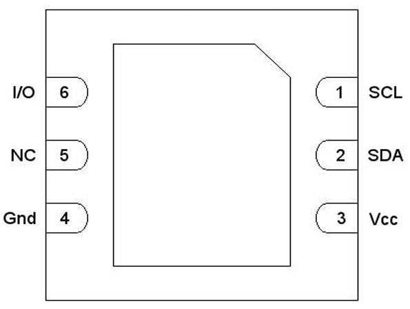
EEPROM
The device is equipped with 2 EEPROM memory modules. EEPROM B is read-only and reserved for the producer's purposes.
EEPROM device
Part number: M24C02-RMC6
EEPROM A connections table
|
EEPROM pin |
Description |
User-space name |
|
1 |
Address pin 0 (GND) |
X |
|
2 |
Address pin 1 (+3V3) |
X |
|
3 |
Address pin 2 (+3V3) |
X |
|
5 |
I2C2 data |
X |
|
6 |
I2C2 clock |
X |
|
7 |
EEPROM write-protect |
gpiochip0 2 |
EEPROM B (EEPROM SN) connections table
|
EEPROM pin |
Description |
User-space name |
|
1 |
Address pin 0 (GND) |
X |
|
2 |
Address pin 1 (+3V3) |
X |
|
3 |
Address pin 2 (GND) |
X |
|
5 |
I2C2 data |
X |
|
6 |
I2C2 clock |
X |
|
7 |
EEPROM write-protect (pull-up) |
X |
EEPROM connection diagram

User-space access
EEPROM device name: /sys/bus/nvmem/devices/1-00561
EEPROM device address: 0x56
I2C2
EEPROMs A and B are connected to the CPU with the I2C2 interface.
FLASH
Part number: W25Q64JVSSIQ
FLASH connections table
|
FLASH pin |
Description |
User-space name |
|
1 |
SPI1_CS0 |
gpiochip2 21 |
|
2 |
SPI1_MISO |
X |
|
3 |
SPI1_WP |
X |
|
5 |
SPI1_MOSI |
X |
|
6 |
SPI1_SCLK |
X |
|
7 |
SPI1_HOLD |
X |
FLASH connection diagram

User-space access
FLASH device name: /dev/mtdblock0
SPI1
FLASH is connected to the CPU with the SPI1 interface.
RTC
The device is equipped with a real-time clock operating at 32.768 kHz with a tolerance of 20 ppm. The RTC clock is connected to a DR2032 battery which serves as its power supply.
RTC device
Part number: DS1338
RTC connection diagram

User-space access
Device name: /sys/class/rtc/rtc0
Device address: 0x68
RTC connections table
|
RTC pin |
Description |
|
1 |
Clock oscillator pin no. 1 |
|
2 |
Clock oscillator pin no. 2 |
|
3 |
Battery power pin |
|
5 |
I2C3 data |
|
6 |
I2C3 clock |
I2C3
The real-time clock is connected to the CPU with the I2C3 interface.
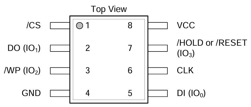
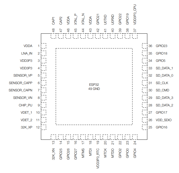
ESP32 microcontroller
The device is equipped with an internal ESP32 microcontroller that can be used for internal purposes.
ESP32 device
Part number: ESP32-DOWD
ESP32 connections table
|
ESP32 pin |
Description |
|
8 |
ESP_P_DETECT |
|
9 |
ESP_CHIP_PU |
|
14 |
ESP32_WDT_EN |
|
15 |
ESP32_WDI |
|
22 |
ESP_GPIO2 |
|
23 |
ESP_GPIO0 |
|
24 |
RESET_WDT |
|
25 |
LED_ESP |
|
26 |
VDD_SDIO |
|
28 |
ESP_SPI_HD |
|
29 |
ESP_SPI_WP |
|
30 |
ESP_SPI_CS0 |
|
31 |
ESP_SPI_CLK |
|
32 |
ESP_SPI_Q |
|
33 |
ESP_SPI_D |
|
38 |
I2C4_SCL |
|
39 |
I2C4_SDA |
|
40 |
ESP_CONSOLE_RX |
|
41 |
ESP_CONSOLE_TX |
ESP32 connections diagram

CPU connections table
|
Signal |
CPU pin |
Default function |
User-space name |
|
ESP_GPIO_0 |
AC14 | GPIO3_IO22 | gpiochip2 22 |
| ESP_GPIO_2 | AC15 | GPIO3_IO20 | gpiochip2 20 |
|
ESP32_WDI |
AF14 | GPIO1_IO01 | gpiochip0 1 |
|
ESP32_WDT_EN |
AF13 |
GPIO1_IO03 |
gpiochip0 3 |
I2C4
The microcontroller is connected to the CPU via the I2C4 interface.
UART3
The microcontroller is connected to the CPU via the UART3 interface.
TPM 2.0
The device is equipped with a trusted platform module in 2.0 standard.
TPM device
Part number: SLM9670
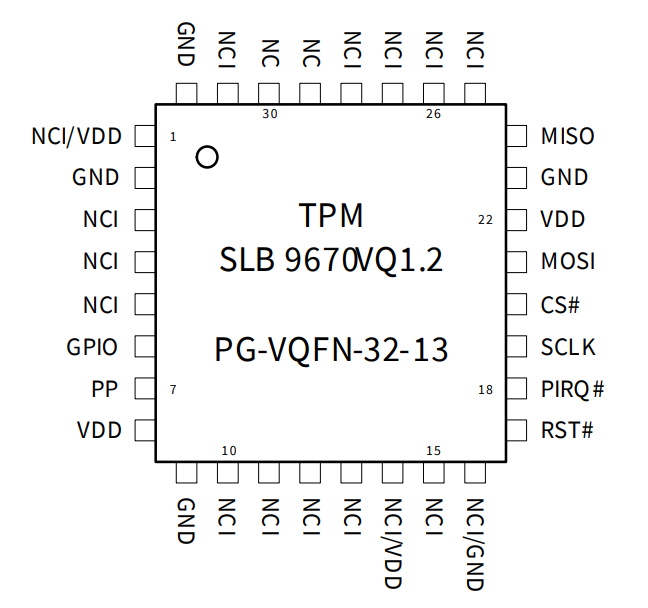
TPM connections table
|
TPM pin |
Description |
|
17 |
Reset |
|
18 |
TPM_IRQ |
|
19 |
SPI2 clock |
|
20 |
SPI2 chip select 0 |
|
21 |
SPI2 master out slave in |
|
24 |
SPI2 master in slave out |
User-space access
Device name: /sys/class/tpm
TPM connection diagram

CPU connections table
|
Signal |
CPU pin |
Default function |
User-space name |
|
TPM_IRQ |
AC24 |
GPIO4_IO23 |
gpiochip3 23 |
|
SPI2_CS0_TPM |
A6 |
GPIO5_IO13 |
gpiochip4 13 |
SPI2
The trusted platform module is connected to the CPU with the SPI2 interface.
Secure element TO136
The device is equipped with a secure element that can be used for data encoding.
Secure element device
Part number: IDEMIA TO136
Secure element connections table
|
Secure element pin |
Description |
|
1 |
I2C4 clock |
|
2 |
I2C4 data |
|
3 |
+3V3 |
|
6 |
IDLE/BUSY state report |
User-space access
Device address: 0x50
Secure element connections diagram

Expander E
The secure element is connected to the Expander E connected to the CPU via the I2C3 interface.
I2C4
The secure element is connected to the CPU via the I2C4 interface.
Buzzer
The device is equipped with a buzzer.
Buzzer device
Part number: LD-BZEG-0905
User-space access
Device name: gpiochip3 7
Label: "BUZZER"
Buzzer connection diagram

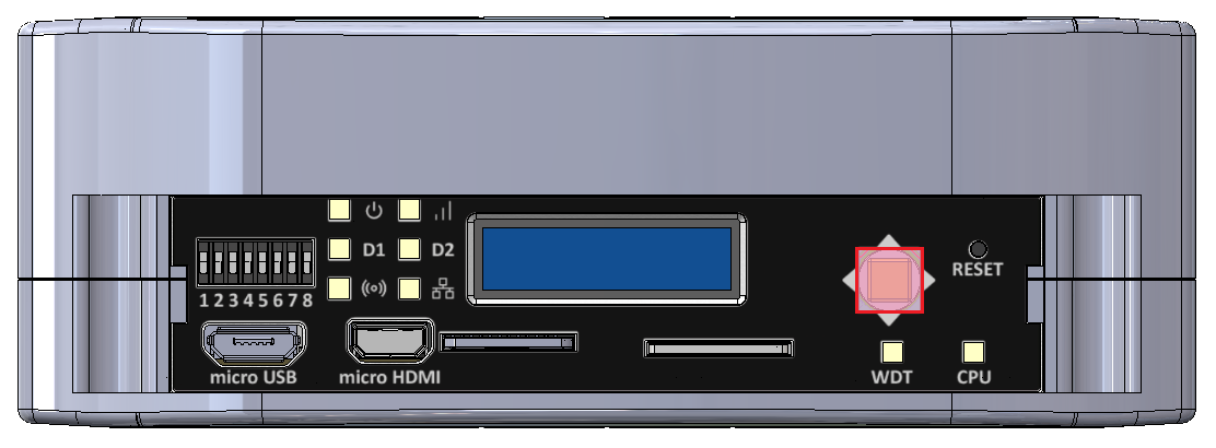
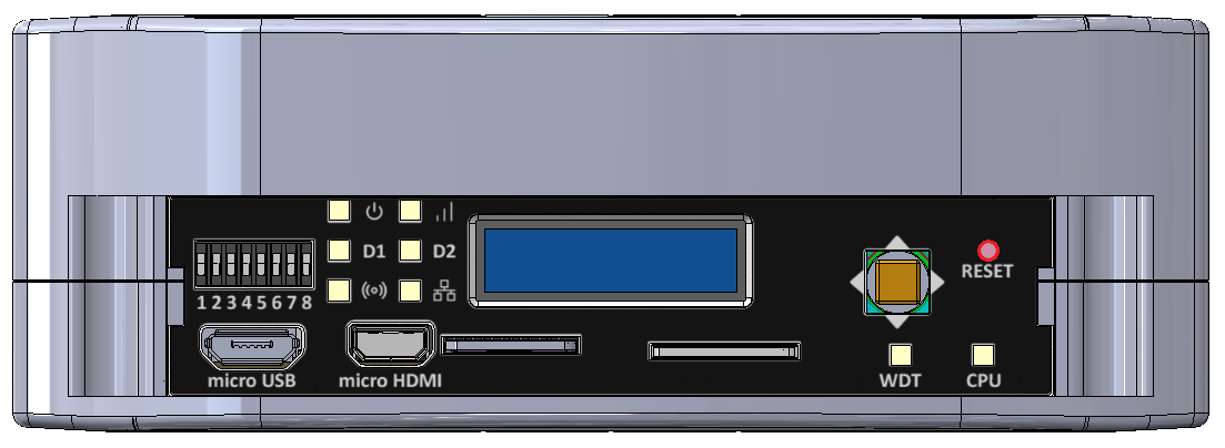
Front Panel
Tiger City IMX Industrial Computer with Linux OS
View of the front panel
Components of the front panel
DIP switches
The device has DIP switches on the front panel which enable the control of various key functions such as:
- booting mode choice
- microUSB signal choice
- choosing Linux console or RS232 signal
- user-written code
DIP switches placement on the front panel
Switch options
|
Switch No. |
Positions |
Description |
|
1 |
OFF - eMMC boot ON - SD card boot |
Boot select - switching between booting device |
|
2 |
OFF - USB1 OTG ON - UART4 (Linux console) |
USB select - microUSB signal choice |
|
3 |
OFF - UART1 (SOM user) ON - UART4 (Linux console) |
RS232 - SOM UART RS232 select |
|
4 |
OFF - UART2 RS232 user ON - ESP32 console |
RS232 - SOM UART RS232/ESP32 select |
|
5 |
Unassigned |
Currently not used |
|
6-8 |
OFF/ON |
User options |
Connections diagram

Expander D
User-defined DIP switch options are connected to the expander D which is connected to the CPU via the I2C3 interface.
USB1
The USB MUX select 1 and the USB MUX select 2 signals are connected to the multiplexer A associated with USB1.
Signal LEDs
The device is equipped with 8 LEDs. 2 of these LEDs are placed on the mainboard, while the other 6 are on the front panel of the HMI board.
LEDs location
LEDs connections
|
Description |
User-space name |
Label |
| Power LED |
gpiochip6 9 |
"LED_5V" |
| CPU LED |
gpiochip0 3 |
"LED_MAINBOARD" |
|
User LED 1 G |
gpiochip6 10 |
"LED3_GREEN" |
|
User LED 1 R |
gpiochip6 5 |
"LED3_RED" |
|
User LED 1 B |
gpiochip6 12 |
"LED3_BLUE" |
|
User LED 2 G |
gpiochip6 13 |
"LED4_GREEN" |
|
User LED 2 R |
gpiochip6 11 |
"LED4_RED" |
|
User LED 2 B |
gpiochip6 15 |
"LED4_BLUE" |
LED connection diagram

ESP32 microcontroller
ESP LED is connected directly to the ESP32 microcontroller.
GSM
GSM LED is connected directly to the GSM modem.
ETHERNET
ETH activity LED and ETH link LED are connected directly to the ETHERNET physical layer.
Expander D
Power LED, User LED 1 and User LED2 are connected to the expander D which is connected to the CPU via the I2C3 interface.
OLED display
The device is equipped with a 0.87” black and white display with a resolution of 128x32 px.
OLED display placement
OLED device
Part number: SCE087002-V01
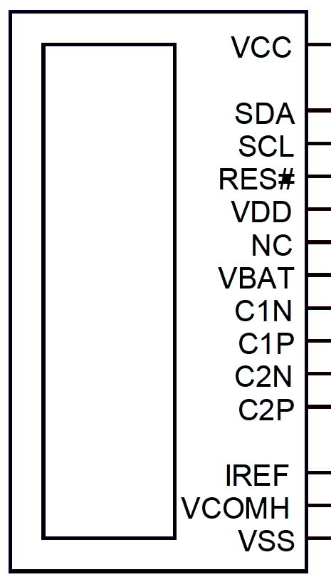
OLED connections table
|
OLED pin |
Description |
User-space name |
|
RES# |
RESET |
X |
|
SCL |
I2C3 clock |
X |
|
SDA |
I2C3 data |
X |
|
VCC |
OLED ON/OFF |
gpiochip6 14, "OLED_EN" |
OLED connections diagram

Expander D
The OLED display is connected to Expander D which is connected to the CPU via the I2C3 interface.
I2C3
The OLED display is directly connected to the CPU via the I2C3 interface.
Joystick
The device is equipped with a joystick for controlling its functions.
Placement
Device
Part number: INT-1500D
Connections table
|
Joystick signal |
Expander D pin |
User-space name |
Label |
|
Right |
20 |
gpiochip6 3 |
"JOY_RIGHT" |
|
Up |
18 |
gpiochip6 1 |
"JOY_UP" |
|
Left |
17 |
gpiochip6 0 |
"JOY_LEFT" |
|
Down |
19 |
gpiochip6 2 |
"JOY_DOWN" |
|
Push |
21 |
gpiochip6 4 |
"JOY_PUSH" |
Connection diagram

Expander D
Joystick is connected to the Expander D which is connected to the CPU via the I2C3 interface.
Reset button
The device has a reset button on the front panel.
Reset button location
Connections diagram

Watchdog + reset
Expanders
Tiger City IMX Industrial Computer with Linux OS
Expander A
Part number: 74HC595BQ
Expander A diagram
Expander A pins description
|
Pin |
Type |
Usage |
User-space name |
Description |
|
1 |
Q1 |
DO1 |
gpiochip8 1 |
Digital output 1 |
|
2 |
Q2 |
DO2 |
gpiochip8 2 |
Digital output 2 |
|
3 |
Q3 |
DO3 |
gpiochip8 3 |
Digital output 3 |
|
4 |
Q4 |
DO4 |
gpiochip8 4 |
Digital output 4 |
|
5 |
Q5 |
DO5 |
gpiochip8 5 |
Digital output 5 |
|
6 |
Q6 |
DO6 |
gpiochip8 6 |
Digital output 6 |
|
7 |
Q7 |
DO7 |
gpiochip8 7 |
Digital output 7 |
|
9 |
Q7S |
NC |
X |
Not connected |
|
10 |
MR/ |
NRST_GLOBAL |
X |
Reset |
|
11 |
SHCP |
SPI1_SCLK |
X |
SPI clock |
|
12 |
STCP |
SPI1_CS1 |
X |
SPI chip select |
|
13 |
OE/ |
GND |
X |
Output enable |
|
14 |
DS |
SPI1_MOSI |
X |
SPI master out slave in |
|
15 |
Q0 |
MUX_DIO_SEL |
gpiochip8 0 |
MUX_PWM selection signal |
|
16 |
VCC |
+3V3 |
X |
Power supply |
SPI1
|
Signal |
Processor pin |
Default function |
|
Chip select 0 |
AD18 |
SPI1_CS0 |
|
Chip select 1 |
AG23 |
SPI1_CS1 |
|
Master in slave out |
A7 |
SPI1_MISO |
|
Clock |
D6 |
SPI1_SCLK |
|
Master out slave in |
B7 |
SPI1_MOSI |
Expander B
Part number: SC16IS752IBS
Expander B diagram
Expander B pins description
|
Pin |
Type |
Usage |
User-space name |
Description |
|
1 |
RXA(I) |
RS485_UART1_RX |
X |
RS485 UART1 RX |
|
2 |
RESET/ |
RS485_NRST |
X |
Reset |
|
3 |
XTAL1(I) |
TXCO_OUT |
X |
Oscillator output |
|
4 |
XTAL2(O) |
NC |
X |
Not connected |
|
5 |
VDD |
+3V3 |
X |
Power supply |
|
6 |
I2C / SPI/ |
GND |
X |
Ground |
|
7 |
CS/ / A0 |
SPI2_CS1 |
X |
SPI chip select |
|
8 |
SI / A1 |
SPI2_MOSI |
X |
SPI master out slave in |
|
9 |
SO |
SPI2_MISO |
X |
SPI master in slave out |
|
10 |
SCL / SCLK |
SPI2_SCLK |
X |
SPI clock |
|
11 |
SDA / VSS |
GND |
X |
Ground |
|
12 |
VSS |
GND |
X |
Ground |
|
14 |
IRQ/ |
RS485_INT |
X |
RS485 interrupt |
|
15 |
CTSB/ |
NC |
X |
Not connected |
|
16 |
RTSB/ |
RS485_UART2_RTS |
X |
RS485 UART2 RTS |
|
17 |
GPIO0 / DSRB/ |
NC |
X |
Not connected |
|
18 |
GPIO1 / DTRB/ |
NC |
X |
Not connected |
|
19 |
GPIO2 / CDB/ |
NC |
X |
Not connected |
|
20 |
GPIO3 / RIB/ |
NC |
X |
Not connected |
|
22 |
TXB(O) |
RS485_UART2_TX |
X |
RS485 UART2 TX |
|
23 |
RXB(I) |
RS485_UART2_RX |
X |
RS485 UART2 RX |
|
24 |
GPIO4 / DSRA/ |
NC |
X |
Not connected |
|
25 |
GPIO5 / DTRA/ |
NC |
X |
Not connected |
|
26 |
GPIO6 / CDA/ |
NC |
X |
Not connected |
|
27 |
GPIO7 / RIA/ |
NC |
X |
Not connected |
|
30 |
RTSA/ |
RS485_UART1_RTS | X | RS485 UART1 RTS |
|
31 |
CTSA/ |
NC |
X |
Not connected |
|
32 |
TXA(O) |
RS485_UART1_TX |
X |
RS485 UART1 TX |
SPI2
|
Signal |
Processor pin |
Default function |
|
Chip select 0 |
A6 |
SPI2_CS0 |
|
Chip select 1 |
AF12 |
SPI2_CS1 |
|
Chip select 2 |
AB19 |
SPI2_CS2 |
|
Master in slave out |
A8 |
SPI2_MISO |
|
Clock |
E6 |
SPI2_SCLK |
|
Master out slave in |
B8 |
SPI2_MOSI |
Expander C
Part number: MCP23017-E/ML
Expander C diagram

Expander C pins description
|
Pin |
Port |
Type |
User-space name |
Description |
|
1 |
GPB4 |
GPIO |
gpiochip5 12 |
UIO4 voltage |
|
2 |
GPB5 |
GPIO |
gpiochip5 13 |
UIO4 current |
|
3 |
GPB6 |
GPIO |
gpiochip5 14 |
UIO4 resistance |
|
4 |
GPB7 |
GPIO |
gpiochip5 15 |
UIO3 resistance |
|
5 |
VDD |
+3V3 |
X |
Power supply |
|
6 |
VSS |
GND |
X |
Ground |
|
7 |
NC |
NC |
X |
Not connected |
|
8 |
SCK |
GPIO |
X |
I2C clock |
|
9 |
SDA |
GPIO |
X |
I2C data |
|
10 |
NC |
NC |
X |
Not connected |
|
11 |
A0 |
GND |
X |
Address bit 0 |
|
12 |
A1 |
GND |
X |
Address bit 1 |
|
13 |
A2 |
GND |
X |
Address bit 2 |
|
14 |
RESET/ |
EXP2_NRST |
X |
Reset |
|
15 |
INTB |
NC |
X |
Not connected |
|
16 |
INTA |
NC |
X |
Not connected |
|
17 |
GPA0 |
GPIO |
gpiochip5 0 |
UIO2 resistance |
|
18 |
GPA1 |
GPIO |
gpiochip5 1 |
UIO1 resistance |
|
19 |
GPA2 |
GPIO |
gpiochip5 2 |
UIO1 voltage |
|
20 |
GPA3 |
GPIO |
gpiochip5 3 |
UIO2 voltage |
|
21 |
GPA4 |
GPIO |
gpiochip5 4 |
UIO3 voltage |
|
22 |
GPA5 |
GPIO |
gpiochip5 5 |
UIO1 current |
|
23 |
GPA6 |
GPO |
gpiochip5 6 |
UIO4 I source |
|
24 |
GPA7 |
GPIO |
gpiochip5 7 |
UIO3 current |
|
25 |
GPB0 |
GPIO |
gpiochip5 8 |
UIO2 current |
|
26 |
GPB1 |
GPO |
gpiochip5 9 |
UIO1 I source |
|
27 |
GPB2 |
GPO |
gpiochip5 10 |
UIO2 I source |
|
28 |
GPB3 |
GPO |
gpiochip5 11 |
UIO3 I source |
I2C2
Device name: /dev/i2c-1
|
Signal |
Processor pin |
Default function |
|
Clock |
D10 |
I2C2_SCL |
|
Data |
D9 |
I2C2_SDA |
Expander D
Part number: MCP23017
Expander D diagram
Expander D pins description
|
Pin |
Port |
Type |
User-space name |
Description |
|
1 |
GPB4 |
GPO |
gpiochip6 12 |
LED3 BLUE ON / OFF |
|
2 |
GPB5 |
GPO |
gpiochip6 13 |
LED4 GREEN ON / OFF |
|
3 |
GPB6 |
GPO |
gpiochip6 14 |
OLED ON / OFF |
|
4 |
GPB7 |
GPO |
gpiochip6 15 |
LED4 BLUE ON / OFF |
|
5 |
VDD |
+3V3 |
X |
Power supply |
|
6 |
VSS |
GND |
X |
Ground |
|
7 |
NC1 |
NC |
X |
Not connected |
|
8 |
SCK |
GPIO |
X |
I2C clock |
|
9 |
SDA |
GPIO |
X |
I2C data |
|
10 |
NC2 |
NC |
X |
Not connected |
|
11 |
A0 |
GND |
X |
Address bit 0 |
|
12 |
A1 |
GND |
X |
Address bit 1 |
|
13 |
A2 |
GND |
X |
Address bit 2 |
|
14 |
RESET/ |
NRST_GLOBAL |
X |
Reset |
|
15 |
INTB |
HMI_IRQ |
X |
Interrupt B |
|
16 |
INTA |
HMI_IRQ |
X |
Interrupt A |
|
17 |
GPA0 |
GPI |
gpiochip6 0 |
Joystick left input |
|
18 |
GPA1 |
GPI |
gpiochip6 1 |
Joystick up input |
|
19 |
GPA2 |
GPI |
gpiochip6 2 |
Joystick down input |
|
20 |
GPA3 |
GPI |
gpiochip6 3 |
Joystick right input |
|
21 |
GPA4 |
GPI |
gpiochip6 4 |
Joystick push input |
|
22 |
GPA5 |
GPO |
gpiochip6 5 |
LED3 RED ON / OFF |
|
23 |
GPA6 |
GPI |
gpiochip6 6 |
DIP switch 6 input |
|
24 |
GPA7 |
GPI |
gpiochip6 7 |
DIP switch 7 input |
|
25 |
GPB0 |
GPI |
gpiochip6 8 |
DIP switch 8 input |
|
26 |
GPB1 |
GPO |
gpiochip6 9 |
LED 5 V power supply ON / OFF |
|
27 |
GPB2 |
GPO |
gpiochip6 10 |
LED3 GREEN ON / OFF |
|
28 |
GPB3 |
GPO |
gpiochip6 11 |
LED4 RED ON / OFF |
I2C3
Device name: /dev/i2c-2
|
Signal |
Processor pin |
Default function |
|
Clock |
E10 |
I2C3_SCL |
|
Data |
F10 |
I2C3_SDA |
Expander E
Part number: MCP23017-E/ML
Expander E diagram

Expander E pins description
|
Pin |
Port |
Type |
User-space name |
Description |
|
1 |
GPB4 |
GPI |
gpiochip5 12 |
Digital input 4 (DIO circuit) |
|
2 |
GPB5 |
GPI |
gpiochip5 13 |
Digital input 5 (DIO circuit) |
|
3 |
GPB6 |
GPI |
gpiochip5 14 |
Digital input 6 (DIO circuit) |
|
4 |
GPB7 |
GPI |
gpiochip5 15 |
Digital input 7 (DIO circuit) |
|
5 |
VDD |
+3V3 |
X |
Power supply |
|
6 |
VSS |
GND |
X |
Ground |
|
7 |
NC |
NC |
X |
Not connected |
|
8 |
SCK |
GPIO |
X |
I2C clock |
|
9 |
SDA |
GPIO |
X |
I2C data |
|
10 |
NC |
NC |
X |
Not connected |
|
11 |
A0 |
+3V3 |
X |
Address bit 0 |
|
12 |
A1 |
+3V3 |
X |
Address bit 1 |
|
13 |
A2 |
GND |
X |
Address bit 2 |
|
14 |
RESET/ |
EXP1_NRST |
X |
Reset |
|
15 |
INTB |
GPIO_EXP_INT |
X |
Interrupt B |
|
16 |
INTA |
GPIO_EXP_INT |
X |
Interrupt A |
|
17 |
GPA0 |
GPO |
gpiochip5 0 |
Termination RS485_4 ON / OFF |
|
18 |
GPA1 |
GPO |
gpiochip5 1 |
Termination RS485_3 ON / OFF |
|
19 |
GPA2 |
GPO |
gpiochip5 2 |
Termination RS485_2 ON / OFF |
|
20 |
GPA3 |
GPO |
gpiochip5 3 |
Termination RS485_1 ON / OFF |
|
21 |
GPA4 |
NC |
X |
Not connected |
|
22 |
GPA5 |
NC |
X |
Not connected |
|
23 |
GPA6 |
GPO |
gpiochip5 6 |
Secure chip idle/busy |
|
24 |
GPA7 |
GPI |
gpiochip5 7 |
Digital input 1 (DIO circuit) |
|
25 |
GPB0 |
GPO |
gpiochip5 8 |
Digital input 2 (DIO circuit) |
|
26 |
GPB1 |
GPI |
gpiochip5 9 |
SD detect |
|
27 |
GPB2 |
GPI |
gpiochip5 10 |
VIN level error |
|
28 |
GPB3 |
GPI |
gpiochip5 11 |
Digital input 3 (DIO circuit) |
I2C3
Device name: /dev/i2c-2
|
Signal |
Processor pin |
Default function |
|
Clock |
E10 |
I2C3_SCL |
|
Data |
F10 |
I2C3_SDA |
Expander F
Part number: SC16IS752IBS
Expander F diagram
Expander F pins description
|
Pin |
Type |
Usage |
User-space name |
Description |
|
1 |
RXA(I) |
RS485_UART4_RX |
X |
RS485 UART4 RX |
|
2 |
RESET/ |
RS485_NRST |
X |
Reset |
|
3 |
XTAL1(I) |
TXCO_OUT |
X |
Oscillator output |
|
4 |
XTAL2(O) |
NC |
X |
Not connected |
|
5 |
VDD |
+3V3 |
X |
Power supply |
|
6 |
I2C / SPI/ |
GND |
X |
Ground |
|
7 |
CS/ / A0 |
SPI2_CS2 |
X |
SPI chip select |
|
8 |
SI / A1 |
SPI2_MOSI |
X |
SPI master out slave in |
|
9 |
SO |
SPI2_MISO |
X |
SPI master in slave out |
|
10 |
SCL / SCLK |
SPI2_SCLK |
X |
SPI clock |
|
11 |
SDA / VSS |
GND |
X |
Ground |
|
12 |
VSS |
GND |
X |
Ground |
|
14 |
IRQ/ |
RS485_INT |
X |
RS485 interrupt |
|
15 |
CTSB/ |
NC |
X |
Not connected |
|
16 |
RTSB/ |
RS485_UART3_RTS |
X |
RS485 UART3 RTS |
|
17 |
GPIO0 / DSRB/ |
NC |
X |
Not connected |
|
18 |
GPIO1 / DTRB/ |
NC |
X |
Not connected |
|
19 |
GPIO2 / CDB/ |
NC |
X |
Not connected |
|
20 |
GPIO3 / RIB/ |
NC |
X |
Not connected |
|
22 |
TXB(O) |
RS485_UART3_TX |
X |
RS485 UART3 TX |
|
23 |
RXB(I) |
RS485_UART3_RX |
X |
RS485 UART3 RX |
|
24 |
GPIO4 / DSRA/ |
NC |
X |
Not connected |
|
25 |
GPIO5 / DTRA/ |
NC |
X |
Not connected |
|
26 |
GPIO6 / CDA/ |
NC |
X |
Not connected |
|
27 |
GPIO7 / RIA/ |
NC |
X |
Not connected |
|
30 |
RTSA/ |
RS485_UART4_RTS | X | RS485 UART4 RTS |
|
31 |
CTSA/ |
NC |
X |
Not connected |
|
32 |
TXA(O) |
RS485_UART4_TX |
X |
RS485 UART4 TX |
SPI2
|
Signal |
Processor pin |
Default function |
|
Chip select 0 |
A6 |
SPI2_CS0 |
|
Chip select 1 |
AF12 |
SPI2_CS1 |
|
Chip select 2 |
AB19 |
SPI2_CS2 |
|
Master in slave out |
A8 |
SPI2_MISO |
|
Clock |
E6 |
SPI2_SCLK |
|
Master out slave in |
B8 |
SPI2_MOSI |
Connectors Designations
Tiger City IMX Industrial Computer with Linux OS
Principle of designating connector pins
Each pin designation is composed of 2 parts.
Part 1
Choose a letter stating the type and purpose of the connector, chosen individually with ease of use by the user in mind.
General connectors
D - digital input pin
H - digital input/output pin
U - universal input/output pin
G - ground potential
RS485
A - A pin of the connector
B - B pin of the connector
RS232
T - Tx pin of the connector
R - Rx pin of the connector
1-Wire
5V - +5 V voltage
1W - 1-Wire data
Part 2
Choose a digit representing the pin on the connector. In case of more than 10 pins on the connectors, letters should be used.
Connector designations for IMX8
|
Eagle designation |
Documentation designation |
|
Digital inputs connectors |
|
|
1 |
G |
|
2 |
D1 |
|
3 |
D2 |
|
4 |
D3 |
|
5 |
D4 |
|
6 |
D5 |
|
Digital inputs/outputs connectors |
|
|
1 |
H1 |
|
2 |
H2 |
|
3 |
H3 |
|
4 |
G |
|
5 |
H4 |
|
6 |
H5 |
|
7 |
H6 |
|
8 |
H7 |
|
Universal inputs/outputs connector |
|
|
1 |
U1 |
|
2 |
U2 |
|
3 |
G |
|
4 |
U3 |
|
5 |
U4 |
|
RS485 1/2 connectors |
|
|
1 |
A1 |
|
2 |
B1 |
|
3 |
G |
|
4 |
A2 |
|
5 |
B2 |
|
RS485 3/4 connectors |
|
|
1 |
A3 |
|
2 |
B3 |
|
3 |
G |
|
4 |
A4 |
|
5 |
B4 |
|
RS232 1/2 & 1-Wire connectors |
|
|
1 |
G |
|
2 |
T1 |
|
3 |
R1 |
|
4 |
T2 |
|
5 |
R2 |
|
6 |
1W |
|
7 |
5V |
|
8 |
G |