| **Connector pin** | **Description** |
| 1 | GND |
| 2 | VIN |
| 3 | GND |
| 4 | SPI1 MOSI |
| 5 | GND |
| 6 | SPI1 SCLK |
| 7 | GND |
| 8 | SPI1 MISO |
| 9 | GND |
| 10 | RTC battery power supply |
| 11 | External watchdog reset |
| 12 | NC |
| 13 | GND |
| 14 | NC |
| 15 | NC |
| 16 | NC |
| 17 | GPIO4 IO25 |
| 18 | GND |
| 19 | GPIO1 IO07 |
| 20 | GPIO4 IO21 |
| 21 | GPIO5 IO09 |
| 22 | Global reset |
| 23 | GND |
| 24 | I2C3 SDA |
| 25 | I2C3 SCL |
| 26 | GND |
| 27 | +3V3 |
| 28 | GND |
| 29 | USB3 positive pole |
| 30 | USB3 negative pole |
| 31 | GND |
| 32 | +20V |
| 33 | UIO reset |
| 34 | NC |
| 35 | NC |
| 36 | +1V8 |
| 37 | +1V8 |
| 38 | GND |
| 39 | +5V |
| 40 | +5V |
| 41 | GND |
| 42 | GND |
| 43 | VIN |
| 44 | GND |
| **Signal** | **Default function** | **User-space name ** | |
| ESP32\_WDI | GPIO1\_IO01 | gpiochip0 1 | ESP32\_WDI |
| SOM\_GLOB\_NRST | GPIO5\_IO02 | gpiochip4 2 | GLOBAL\_NRST |
| GPIO0 | GPIO3\_IO22 | gpiochip2 22 | ESP\_GPIO0 |
| GPIO2 | GPIO3\_IO20 | gpiochip2 20 | ESP\_GPIO2 |
| ESP\_CHIP\_PU | GPIO4\_IO20 | gpiochip3 20 | ESP\_CHIP\_PU |
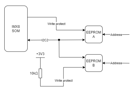
| **EEPROM pin** | **Description** | **User-space name** |
| 1 | Address pin 0 (GND) | X |
| 2 | Address pin 1 (+3V3) | X |
| 3 | Address pin 2 (+3V3) | X |
| 5 | I2C2 data | X |
| 6 | I2C2 clock | X |
| 7 | EEPROM write-protect | gpiochip0 2 |
| **EEPROM pin** | **Description** | **User-space name** |
| 1 | Address pin 0 (GND) | X |
| 2 | Address pin 1 (+3V3) | X |
| 3 | Address pin 2 (GND) | X |
| 5 | I2C2 data | X |
| 6 | I2C2 clock | X |
| 7 | EEPROM write-protect (pull-up) | X |
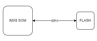
| **FLASH pin** | **Description** | **User-space name** |
| 1 | SPI1\_CS0 | gpiochip2 21 |
| 2 | SPI1\_MISO | X |
| 3 | SPI1\_WP | X |
| 5 | SPI1\_MOSI | X |
| 6 | SPI1\_SCLK | X |
| 7 | SPI1\_HOLD | X |
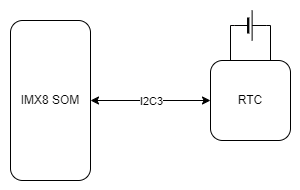
| **RTC pin** | **Description** |
| 1 | Clock oscillator pin no. 1 |
| 2 | Clock oscillator pin no. 2 |
| 3 | Battery power pin |
| 5 | I2C3 data |
| 6 | I2C3 clock |
| **ESP32 pin** | **Description** |
| 8 | ESP\_P\_DETECT |
| 9 | ESP\_CHIP\_PU |
| 14 | ESP32\_WDT\_EN |
| 15 | ESP32\_WDI |
| 22 | ESP\_GPIO2 |
| 23 | ESP\_GPIO0 |
| 24 | RESET\_WDT |
| 25 | LED\_ESP |
| 26 | VDD\_SDIO |
| 28 | ESP\_SPI\_HD |
| 29 | ESP\_SPI\_WP |
| 30 | ESP\_SPI\_CS0 |
| 31 | ESP\_SPI\_CLK |
| 32 | ESP\_SPI\_Q |
| 33 | ESP\_SPI\_D |
| 38 | I2C4\_SCL |
| 39 | I2C4\_SDA |
| 40 | ESP\_CONSOLE\_RX |
| 41 | ESP\_CONSOLE\_TX |
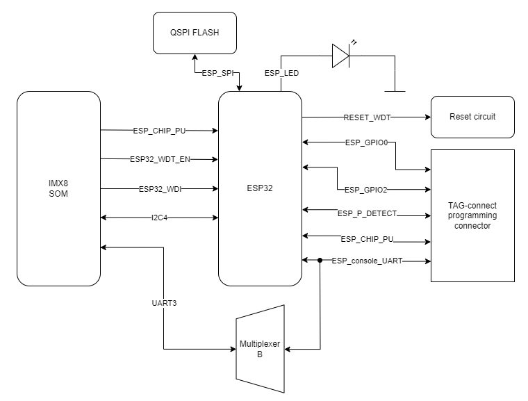
| **Signal** | **CPU pin** | **Default function** | **User-space name** |
| ESP\_GPIO\_0 | AC14 | GPIO3\_IO22 | gpiochip2 22 |
| ESP\_GPIO\_2 | AC15 | GPIO3\_IO20 | gpiochip2 20 |
| ESP32\_WDI | AF14 | GPIO1\_IO01 | gpiochip0 1 |
| ESP32\_WDT\_EN | AF13 | GPIO1\_IO03 | gpiochip0 3 |
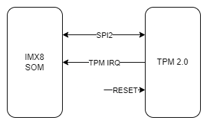
| **TPM pin** | **Description** |
| 17 | Reset |
| 18 | TPM\_IRQ |
| 19 | SPI2 clock |
| 20 | SPI2 chip select 0 |
| 21 | SPI2 master out slave in |
| 24 | SPI2 master in slave out |
| **Signal** | **CPU pin** | **Default function** | **User-space name** |
| TPM\_IRQ | AC24 | GPIO4\_IO23 | gpiochip3 23 |
| SPI2\_CS0\_TPM | A6 | GPIO5\_IO13 | gpiochip4 13 |
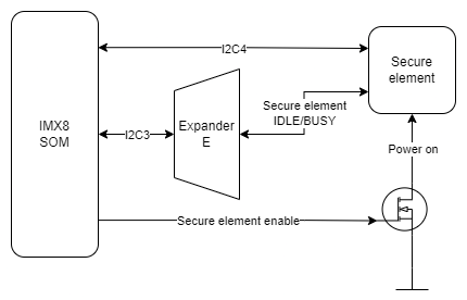
| **Secure element pin** | **Description** |
| 1 | I2C4 clock |
| 2 | I2C4 data |
| 3 | +3V3 |
| 6 | IDLE/BUSY state report |