| **Description** | **Processor pin** | **Default function** |
| 5 V USB voltage | F22 | USB1\_VBUS |
| USB data differential pair negative | A22 | USB1\_D\_N |
| USB data differential pair positive | B22 | USB1\_D\_P |
| USB on the go | AB10 | USB1\_OTG\_PWR |
| **Description** | **Processor pin** | **Default function** |
| USB power switch control | F23 | USB2\_VBUS |
| USB data differential pair negative | A23 | USB2\_D\_N |
| USB data differential pair positive | B23 | USB2\_D\_P |
| **Connector pin** | **Description** |
| A1 | RS485 A1 |
| B1 | RS485 B1 |
| G | Ground |
| A2 | RS485 A2 |
| B2 | RS485 B2 |
| **Connector pin** | **Description** |
| A3 | RS485 A3 |
| B3 | RS485 B3 |
| G | Ground |
| A4 | RS485 A4 |
| B4 | RS485 B4 |
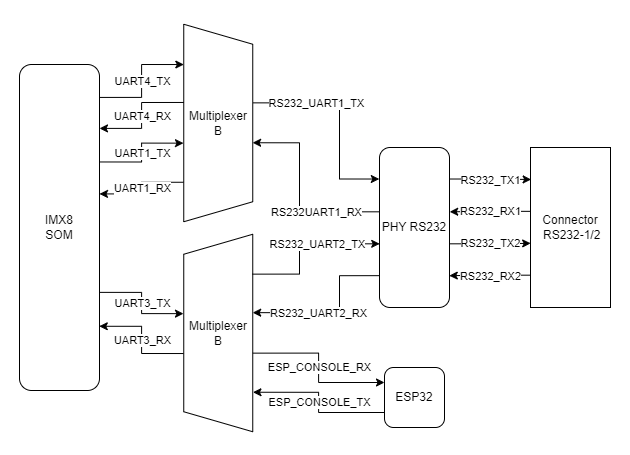
| **Connector pin** | **Description** |
| T1 | RS232 TX1 |
| R1 | RS232 RX1 |
| G | Ground |
| T2 | RS232 TX2 |
| R2 | RS232 RX2 |
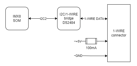
| **Connector pin** | **Description** |
| 1W | 1-Wire data |
| 5V | 1-Wire +5 V power |
| G | Ground |
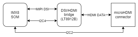
| **Signal** | **Processor pin** | **Default function** |
| DSI\_TX0\_N | A9 | MIPI\_DSI\_TX0\_N |
| DSI\_TX0\_P | B9 | MIPI\_DSI\_TX0\_P |
| DSI\_TX1\_N | A10 | MIPI\_DSI\_TX1\_N |
| DSI\_TX1\_P | B10 | MIPI\_DSI\_TX1\_P |
| DSI\_TX2\_N | A12 | MIPI\_DSI\_TX2\_N |
| DSI\_TX2\_P | B12 | MIPI\_DSI\_TX2\_P |
| DSI\_TX3\_N | A13 | MIPI\_DSI\_TX3\_N |
| DSI\_TX3\_P | B13 | MIPI\_DSI\_TX3\_P |
| DSI\_CLK\_N | A11 | MIPI\_DSI\_CLK\_N |
| DSI\_CLK\_P | B11 | MIPI\_DSI\_CLK\_P |
| **Function** | **Processor pin** | **Default function** |
| USB power switch control | F23 | USB2\_VBUS |
| USB data differential pair negative | A23 | USB2\_D\_N |
| USB data differential pair positive | B23 | USB2\_D\_P |
| **Function** | **Processor pin** | **Default function** |
| SD data line 0 | AB23 | SD2\_DATA0 |
| SD data line 1 | AB24 | SD2\_DATA1 |
| SD data line 2 | V24 | SD2\_DATA2 |
| SD data line 3 | V23 | SD2\_DATA3 |
| SD command line | W24 | SD2\_CMD |
| SD clock | W23 | SD2\_CLK |
| **DI connector pin** | **Processor pin** | **User-space name** | |
| DI1 | AC22 | gpiochip3 26 | "DI1" |
| DI2 | AD23 | gpiochip3 24 | "DI2" |
| DI3 | AB22 | gpiochip3 22 | "DI3" |
| DI4 | AD15 | gpiochip2 25 | "DI4" |
| DI5 | AC13 | gpiochip2 24 | "DI5" |
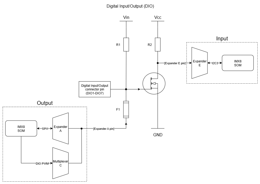
| **DIO connector pin** | **Input** | **Output** | ||
| **User-space name** | **Expander E pin** | **User-space name** | **Expander A pin** | |
| DIO1 | gpiochip5 9 | 24 | gpiochip7 1 | 1 |
| DIO2 | gpiochip5 10 | 25 | gpiochip7 2 | 2 |
| DIO3 | gpiochip5 11 | 28 | gpiochip7 3 | 3 |
| DIO4 | gpiochip5 12 | 1 | gpiochip7 4 | 4 |
| DIO5 | gpiochip5 13 | 2 | gpiochip7 5 | 5 |
| DIO6 | gpiochip5 14 | 3 | gpiochip7 6 | 6 |
| DIO7 | gpiochip5 15 | 4 | gpiochip7 7 | 7 |
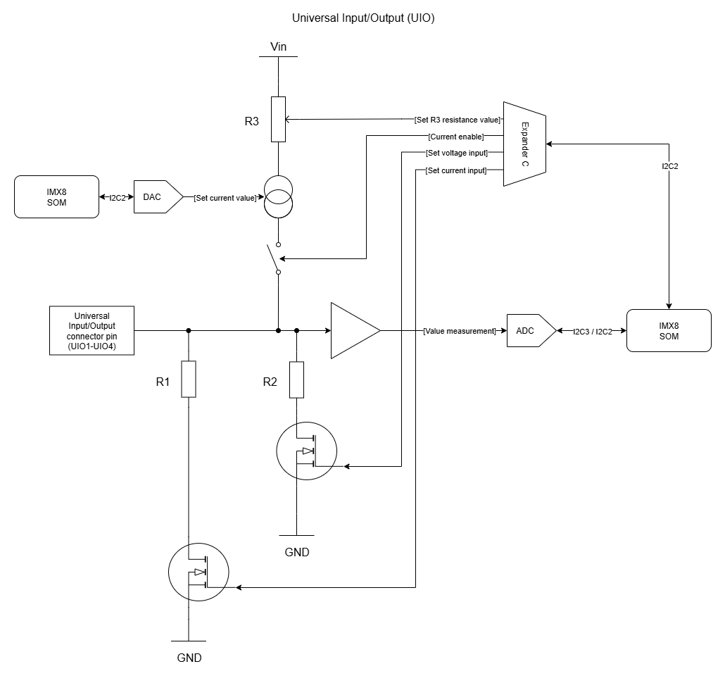
| **Configuration signal** | **Modes of operation** | |||
|---|---|---|---|---|
| **DI dry contact** | **AI 0-10 V** | **AI 0-4-20 mA** | **AO 4-20 mA / temperature\* / resistance** | |
| Set voltage input | 0 | 1 | 0 | 0 |
| Set current input | 0 | 1 | 0 | 1 |
| Current enable | 1 | 0 | 0 | 1 |
| Set R3 resistance value | 1 | X | X | 1 or 0\*\* |
| Set current value | 12-bit value\*\*\* | X | X | 12-bit value\*\*\* |
| **UIO connector pin** | **Configuration signal** | **Expander C pin** |
| UIO1 | Current enable | 20 |
| Set voltage input | 19 | |
| Set current input | 27 | |
| Set R3 resistance value | 21 | |
| UIO2 | Current enable | 3 |
| Set voltage input | 22 | |
| Set current input | 28 | |
| Set R3 resistance value | 4 | |
| UIO3 | Current enable | 23 |
| Set voltage input | 17 | |
| Set current input | 1 | |
| Set R3 resistance value | 18 | |
| UIO4 | Current enable | 26 |
| Set voltage input | 24 | |
| Set current input | 2 | |
| Set R3 resistance value | 25 |
| **Connector pin** | **Description** |
| 1 | GND |
| 2 | VIN |
| 3 | GND |
| 4 | SPI1 MOSI |
| 5 | GND |
| 6 | SPI1 SCLK |
| 7 | GND |
| 8 | SPI1 MISO |
| 9 | GND |
| 10 | RTC battery power supply |
| 11 | External watchdog reset |
| 12 | NC |
| 13 | GND |
| 14 | NC |
| 15 | NC |
| 16 | NC |
| 17 | GPIO4 IO25 |
| 18 | GND |
| 19 | GPIO1 IO07 |
| 20 | GPIO4 IO21 |
| 21 | GPIO5 IO09 |
| 22 | Global reset |
| 23 | GND |
| 24 | I2C3 SDA |
| 25 | I2C3 SCL |
| 26 | GND |
| 27 | +3V3 |
| 28 | GND |
| 29 | USB3 positive pole |
| 30 | USB3 negative pole |
| 31 | GND |
| 32 | +20V |
| 33 | UIO reset |
| 34 | NC |
| 35 | NC |
| 36 | +1V8 |
| 37 | +1V8 |
| 38 | GND |
| 39 | +5V |
| 40 | +5V |
| 41 | GND |
| 42 | GND |
| 43 | VIN |
| 44 | GND |
| **Signal** | **Default function** | **User-space name ** | |
| ESP32\_WDI | GPIO1\_IO01 | gpiochip0 1 | ESP32\_WDI |
| SOM\_GLOB\_NRST | GPIO5\_IO02 | gpiochip4 2 | GLOBAL\_NRST |
| GPIO0 | GPIO3\_IO22 | gpiochip2 22 | ESP\_GPIO0 |
| GPIO2 | GPIO3\_IO20 | gpiochip2 20 | ESP\_GPIO2 |
| ESP\_CHIP\_PU | GPIO4\_IO20 | gpiochip3 20 | ESP\_CHIP\_PU |
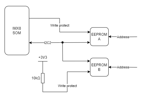
| **EEPROM pin** | **Description** | **User-space name** |
| 1 | Address pin 0 (GND) | X |
| 2 | Address pin 1 (+3V3) | X |
| 3 | Address pin 2 (+3V3) | X |
| 5 | I2C2 data | X |
| 6 | I2C2 clock | X |
| 7 | EEPROM write-protect | gpiochip0 2 |
| **EEPROM pin** | **Description** | **User-space name** |
| 1 | Address pin 0 (GND) | X |
| 2 | Address pin 1 (+3V3) | X |
| 3 | Address pin 2 (GND) | X |
| 5 | I2C2 data | X |
| 6 | I2C2 clock | X |
| 7 | EEPROM write-protect (pull-up) | X |
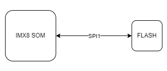
| **FLASH pin** | **Description** | **User-space name** |
| 1 | SPI1\_CS0 | gpiochip2 21 |
| 2 | SPI1\_MISO | X |
| 3 | SPI1\_WP | X |
| 5 | SPI1\_MOSI | X |
| 6 | SPI1\_SCLK | X |
| 7 | SPI1\_HOLD | X |
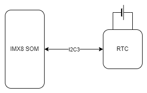
| **RTC pin** | **Description** |
| 1 | Clock oscillator pin no. 1 |
| 2 | Clock oscillator pin no. 2 |
| 3 | Battery power pin |
| 5 | I2C3 data |
| 6 | I2C3 clock |
| **ESP32 pin** | **Description** |
| 8 | ESP\_P\_DETECT |
| 9 | ESP\_CHIP\_PU |
| 14 | ESP32\_WDT\_EN |
| 15 | ESP32\_WDI |
| 22 | ESP\_GPIO2 |
| 23 | ESP\_GPIO0 |
| 24 | RESET\_WDT |
| 25 | LED\_ESP |
| 26 | VDD\_SDIO |
| 28 | ESP\_SPI\_HD |
| 29 | ESP\_SPI\_WP |
| 30 | ESP\_SPI\_CS0 |
| 31 | ESP\_SPI\_CLK |
| 32 | ESP\_SPI\_Q |
| 33 | ESP\_SPI\_D |
| 38 | I2C4\_SCL |
| 39 | I2C4\_SDA |
| 40 | ESP\_CONSOLE\_RX |
| 41 | ESP\_CONSOLE\_TX |
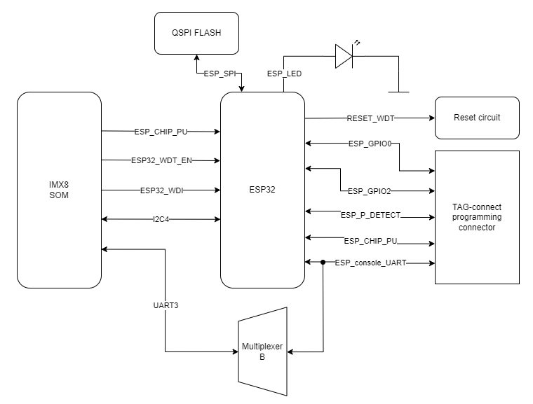
| **Signal** | **CPU pin** | **Default function** | **User-space name** |
| ESP\_GPIO\_0 | AC14 | GPIO3\_IO22 | gpiochip2 22 |
| ESP\_GPIO\_2 | AC15 | GPIO3\_IO20 | gpiochip2 20 |
| ESP32\_WDI | AF14 | GPIO1\_IO01 | gpiochip0 1 |
| ESP32\_WDT\_EN | AF13 | GPIO1\_IO03 | gpiochip0 3 |
| **TPM pin** | **Description** |
| 17 | Reset |
| 18 | TPM\_IRQ |
| 19 | SPI2 clock |
| 20 | SPI2 chip select 0 |
| 21 | SPI2 master out slave in |
| 24 | SPI2 master in slave out |
| **Signal** | **CPU pin** | **Default function** | **User-space name** |
| TPM\_IRQ | AC24 | GPIO4\_IO23 | gpiochip3 23 |
| SPI2\_CS0\_TPM | A6 | GPIO5\_IO13 | gpiochip4 13 |
| **Secure element pin** | **Description** |
| 1 | I2C4 clock |
| 2 | I2C4 data |
| 3 | +3V3 |
| 6 | IDLE/BUSY state report |
| **Switch No.** | **Positions** | **Description** |
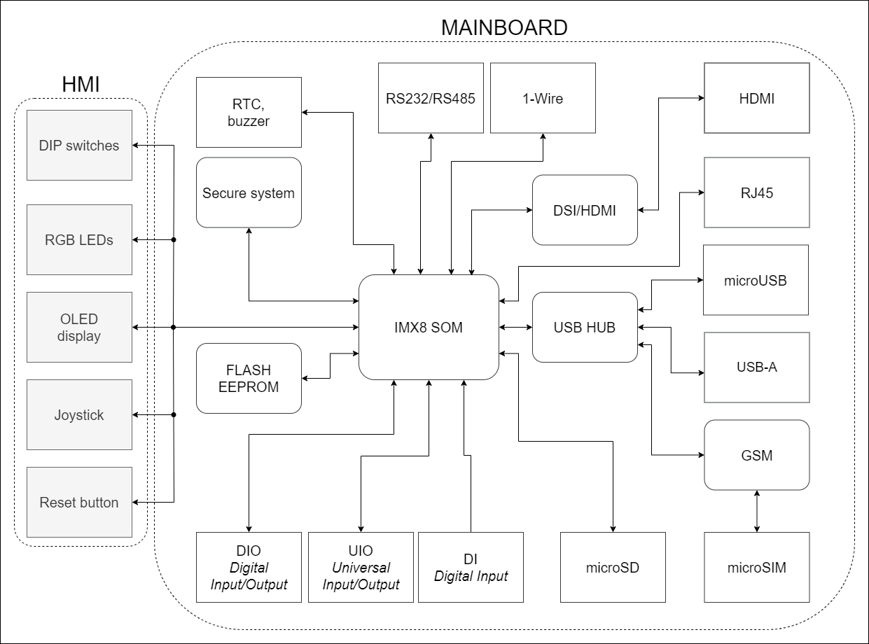
| 1 | OFF - eMMC boot ON - SD card boot | Boot select - switching between booting device |
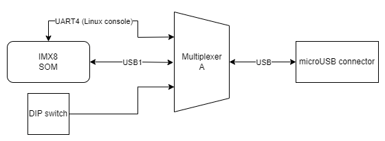
| 2 | OFF - USB1 OTG ON - UART4 (Linux console) | USB select - microUSB signal choice |
| 3 | OFF - UART1 (SOM user) ON - UART4 (Linux console) | RS232 - SOM UART RS232 select |
| 4 | OFF - UART2 RS232 user ON - ESP32 console | RS232 - SOM UART RS232/ESP32 select |
| 5 | Unassigned | Currently not used |
| 6-8 | OFF/ON | User options |
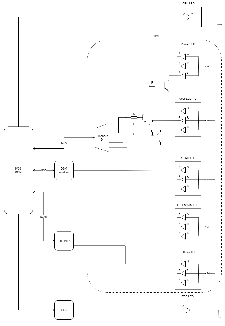
| **Description** | **User-space name** | **Label** |
| Power LED | gpiochip6 9 | "LED\_5V" |
| CPU LED | gpiochip0 3 | "LED\_MAINBOARD" |
| User LED 1 G | gpiochip6 10 | "LED3\_GREEN" |
| User LED 1 R | gpiochip6 5 | "LED3\_RED" |
| User LED 1 B | gpiochip6 12 | "LED3\_BLUE" |
| User LED 2 G | gpiochip6 13 | "LED4\_GREEN" |
| User LED 2 R | gpiochip6 11 | "LED4\_RED" |
| User LED 2 B | gpiochip6 15 | "LED4\_BLUE" |
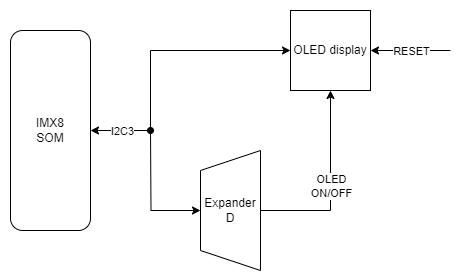
| **OLED pin** | **Description** | **User-space name** |
| RES# | RESET | X |
| SCL | I2C3 clock | X |
| SDA | I2C3 data | X |
| VCC | OLED ON/OFF | gpiochip6 14, "OLED\_EN" |
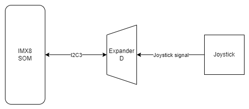
| **Joystick signal** | **Expander D pin** | **User-space name** | **Label** |
| Right | 20 | gpiochip6 3 | "JOY\_RIGHT" |
| Up | 18 | gpiochip6 1 | "JOY\_UP" |
| Left | 17 | gpiochip6 0 | "JOY\_LEFT" |
| Down | 19 | gpiochip6 2 | "JOY\_DOWN" |
| Push | 21 | gpiochip6 4 | "JOY\_PUSH" |
| **Pin** | **Type** | **Usage** | **User-space name** | **Description** |
| 1 | Q1 | DO1 | gpiochip8 1 | Digital output 1 |
| 2 | Q2 | DO2 | gpiochip8 2 | Digital output 2 |
| 3 | Q3 | DO3 | gpiochip8 3 | Digital output 3 |
| 4 | Q4 | DO4 | gpiochip8 4 | Digital output 4 |
| 5 | Q5 | DO5 | gpiochip8 5 | Digital output 5 |
| 6 | Q6 | DO6 | gpiochip8 6 | Digital output 6 |
| 7 | Q7 | DO7 | gpiochip8 7 | Digital output 7 |
| 9 | Q7S | NC | X | Not connected |
| 10 | MR/ | NRST\_GLOBAL | X | Reset |
| 11 | SHCP | SPI1\_SCLK | X | SPI clock |
| 12 | STCP | SPI1\_CS1 | X | SPI chip select |
| 13 | OE/ | GND | X | Output enable |
| 14 | DS | SPI1\_MOSI | X | SPI master out slave in |
| 15 | Q0 | MUX\_DIO\_SEL | gpiochip8 0 | MUX\_PWM selection signal |
| 16 | VCC | +3V3 | X | Power supply |
| **Pin** | **Type** | **Usage** | **User-space name** | **Description** |
| 1 | RXA(I) | RS485\_UART1\_RX | X | RS485 UART1 RX |
| 2 | RESET/ | RS485\_NRST | X | Reset |
| 3 | XTAL1(I) | TXCO\_OUT | X | Oscillator output |
| 4 | XTAL2(O) | NC | X | Not connected |
| 5 | VDD | +3V3 | X | Power supply |
| 6 | I2C / SPI/ | GND | X | Ground |
| 7 | CS/ / A0 | SPI2\_CS1 | X | SPI chip select |
| 8 | SI / A1 | SPI2\_MOSI | X | SPI master out slave in |
| 9 | SO | SPI2\_MISO | X | SPI master in slave out |
| 10 | SCL / SCLK | SPI2\_SCLK | X | SPI clock |
| 11 | SDA / VSS | GND | X | Ground |
| 12 | VSS | GND | X | Ground |
| 14 | IRQ/ | RS485\_INT | X | RS485 interrupt |
| 15 | CTSB/ | NC | X | Not connected |
| 16 | RTSB/ | RS485\_UART2\_RTS | X | RS485 UART2 RTS |
| 17 | GPIO0 / DSRB/ | NC | X | Not connected |
| 18 | GPIO1 / DTRB/ | NC | X | Not connected |
| 19 | GPIO2 / CDB/ | NC | X | Not connected |
| 20 | GPIO3 / RIB/ | NC | X | Not connected |
| 22 | TXB(O) | RS485\_UART2\_TX | X | RS485 UART2 TX |
| 23 | RXB(I) | RS485\_UART2\_RX | X | RS485 UART2 RX |
| 24 | GPIO4 / DSRA/ | NC | X | Not connected |
| 25 | GPIO5 / DTRA/ | NC | X | Not connected |
| 26 | GPIO6 / CDA/ | NC | X | Not connected |
| 27 | GPIO7 / RIA/ | NC | X | Not connected |
| 30 | RTSA/ | RS485\_UART1\_RTS | X | RS485 UART1 RTS |
| 31 | CTSA/ | NC | X | Not connected |
| 32 | TXA(O) | RS485\_UART1\_TX | X | RS485 UART1 TX |
| **Pin** | **Port** | **Type** | **User-space name** | **Description** |
| 1 | GPB4 | GPIO | gpiochip5 12 | UIO4 voltage |
| 2 | GPB5 | GPIO | gpiochip5 13 | UIO4 current |
| 3 | GPB6 | GPIO | gpiochip5 14 | UIO4 resistance |
| 4 | GPB7 | GPIO | gpiochip5 15 | UIO3 resistance |
| 5 | VDD | +3V3 | X | Power supply |
| 6 | VSS | GND | X | Ground |
| 7 | NC | NC | X | Not connected |
| 8 | SCK | GPIO | X | I2C clock |
| 9 | SDA | GPIO | X | I2C data |
| 10 | NC | NC | X | Not connected |
| 11 | A0 | GND | X | Address bit 0 |
| 12 | A1 | GND | X | Address bit 1 |
| 13 | A2 | GND | X | Address bit 2 |
| 14 | RESET/ | EXP2\_NRST | X | Reset |
| 15 | INTB | NC | X | Not connected |
| 16 | INTA | NC | X | Not connected |
| 17 | GPA0 | GPIO | gpiochip5 0 | UIO2 resistance |
| 18 | GPA1 | GPIO | gpiochip5 1 | UIO1 resistance |
| 19 | GPA2 | GPIO | gpiochip5 2 | UIO1 voltage |
| 20 | GPA3 | GPIO | gpiochip5 3 | UIO2 voltage |
| 21 | GPA4 | GPIO | gpiochip5 4 | UIO3 voltage |
| 22 | GPA5 | GPIO | gpiochip5 5 | UIO1 current |
| 23 | GPA6 | GPO | gpiochip5 6 | UIO4 I source |
| 24 | GPA7 | GPIO | gpiochip5 7 | UIO3 current |
| 25 | GPB0 | GPIO | gpiochip5 8 | UIO2 current |
| 26 | GPB1 | GPO | gpiochip5 9 | UIO1 I source |
| 27 | GPB2 | GPO | gpiochip5 10 | UIO2 I source |
| 28 | GPB3 | GPO | gpiochip5 11 | UIO3 I source |
| **Pin** | **Port** | **Type** | **User-space name** | **Description** |
| 1 | GPB4 | GPO | gpiochip6 12 | LED3 BLUE ON / OFF |
| 2 | GPB5 | GPO | gpiochip6 13 | LED4 GREEN ON / OFF |
| 3 | GPB6 | GPO | gpiochip6 14 | OLED ON / OFF |
| 4 | GPB7 | GPO | gpiochip6 15 | LED4 BLUE ON / OFF |
| 5 | VDD | +3V3 | X | Power supply |
| 6 | VSS | GND | X | Ground |
| 7 | NC1 | NC | X | Not connected |
| 8 | SCK | GPIO | X | I2C clock |
| 9 | SDA | GPIO | X | I2C data |
| 10 | NC2 | NC | X | Not connected |
| 11 | A0 | GND | X | Address bit 0 |
| 12 | A1 | GND | X | Address bit 1 |
| 13 | A2 | GND | X | Address bit 2 |
| 14 | RESET/ | NRST\_GLOBAL | X | Reset |
| 15 | INTB | HMI\_IRQ | X | Interrupt B |
| 16 | INTA | HMI\_IRQ | X | Interrupt A |
| 17 | GPA0 | GPI | gpiochip6 0 | Joystick left input |
| 18 | GPA1 | GPI | gpiochip6 1 | Joystick up input |
| 19 | GPA2 | GPI | gpiochip6 2 | Joystick down input |
| 20 | GPA3 | GPI | gpiochip6 3 | Joystick right input |
| 21 | GPA4 | GPI | gpiochip6 4 | Joystick push input |
| 22 | GPA5 | GPO | gpiochip6 5 | LED3 RED ON / OFF |
| 23 | GPA6 | GPI | gpiochip6 6 | DIP switch 6 input |
| 24 | GPA7 | GPI | gpiochip6 7 | DIP switch 7 input |
| 25 | GPB0 | GPI | gpiochip6 8 | DIP switch 8 input |
| 26 | GPB1 | GPO | gpiochip6 9 | LED 5 V power supply ON / OFF |
| 27 | GPB2 | GPO | gpiochip6 10 | LED3 GREEN ON / OFF |
| 28 | GPB3 | GPO | gpiochip6 11 | LED4 RED ON / OFF |
| **Pin** | **Port** | **Type** | **User-space name** | **Description** |
| 1 | GPB4 | GPI | gpiochip5 12 | Digital input 4 (DIO circuit) |
| 2 | GPB5 | GPI | gpiochip5 13 | Digital input 5 (DIO circuit) |
| 3 | GPB6 | GPI | gpiochip5 14 | Digital input 6 (DIO circuit) |
| 4 | GPB7 | GPI | gpiochip5 15 | Digital input 7 (DIO circuit) |
| 5 | VDD | +3V3 | X | Power supply |
| 6 | VSS | GND | X | Ground |
| 7 | NC | NC | X | Not connected |
| 8 | SCK | GPIO | X | I2C clock |
| 9 | SDA | GPIO | X | I2C data |
| 10 | NC | NC | X | Not connected |
| 11 | A0 | +3V3 | X | Address bit 0 |
| 12 | A1 | +3V3 | X | Address bit 1 |
| 13 | A2 | GND | X | Address bit 2 |
| 14 | RESET/ | EXP1\_NRST | X | Reset |
| 15 | INTB | GPIO\_EXP\_INT | X | Interrupt B |
| 16 | INTA | GPIO\_EXP\_INT | X | Interrupt A |
| 17 | GPA0 | GPO | gpiochip5 0 | Termination RS485\_4 ON / OFF |
| 18 | GPA1 | GPO | gpiochip5 1 | Termination RS485\_3 ON / OFF |
| 19 | GPA2 | GPO | gpiochip5 2 | Termination RS485\_2 ON / OFF |
| 20 | GPA3 | GPO | gpiochip5 3 | Termination RS485\_1 ON / OFF |
| 21 | GPA4 | NC | X | Not connected |
| 22 | GPA5 | NC | X | Not connected |
| 23 | GPA6 | GPO | gpiochip5 6 | Secure chip idle/busy |
| 24 | GPA7 | GPI | gpiochip5 7 | Digital input 1 (DIO circuit) |
| 25 | GPB0 | GPO | gpiochip5 8 | Digital input 2 (DIO circuit) |
| 26 | GPB1 | GPI | gpiochip5 9 | SD detect |
| 27 | GPB2 | GPI | gpiochip5 10 | VIN level error |
| 28 | GPB3 | GPI | gpiochip5 11 | Digital input 3 (DIO circuit) |
| **Pin** | **Type** | **Usage** | **User-space name** | **Description** |
| 1 | RXA(I) | RS485\_UART4\_RX | X | RS485 UART4 RX |
| 2 | RESET/ | RS485\_NRST | X | Reset |
| 3 | XTAL1(I) | TXCO\_OUT | X | Oscillator output |
| 4 | XTAL2(O) | NC | X | Not connected |
| 5 | VDD | +3V3 | X | Power supply |
| 6 | I2C / SPI/ | GND | X | Ground |
| 7 | CS/ / A0 | SPI2\_CS2 | X | SPI chip select |
| 8 | SI / A1 | SPI2\_MOSI | X | SPI master out slave in |
| 9 | SO | SPI2\_MISO | X | SPI master in slave out |
| 10 | SCL / SCLK | SPI2\_SCLK | X | SPI clock |
| 11 | SDA / VSS | GND | X | Ground |
| 12 | VSS | GND | X | Ground |
| 14 | IRQ/ | RS485\_INT | X | RS485 interrupt |
| 15 | CTSB/ | NC | X | Not connected |
| 16 | RTSB/ | RS485\_UART3\_RTS | X | RS485 UART3 RTS |
| 17 | GPIO0 / DSRB/ | NC | X | Not connected |
| 18 | GPIO1 / DTRB/ | NC | X | Not connected |
| 19 | GPIO2 / CDB/ | NC | X | Not connected |
| 20 | GPIO3 / RIB/ | NC | X | Not connected |
| 22 | TXB(O) | RS485\_UART3\_TX | X | RS485 UART3 TX |
| 23 | RXB(I) | RS485\_UART3\_RX | X | RS485 UART3 RX |
| 24 | GPIO4 / DSRA/ | NC | X | Not connected |
| 25 | GPIO5 / DTRA/ | NC | X | Not connected |
| 26 | GPIO6 / CDA/ | NC | X | Not connected |
| 27 | GPIO7 / RIA/ | NC | X | Not connected |
| 30 | RTSA/ | RS485\_UART4\_RTS | X | RS485 UART4 RTS |
| 31 | CTSA/ | NC | X | Not connected |
| 32 | TXA(O) | RS485\_UART4\_TX | X | RS485 UART4 TX |
| **Eagle designation** | **Documentation designation** |
| **Digital inputs connectors** | |
| 1 | G |
| 2 | D1 |
| 3 | D2 |
| 4 | D3 |
| 5 | D4 |
| 6 | D5 |
| **Digital inputs/outputs connectors** | |
| 1 | H1 |
| 2 | H2 |
| 3 | H3 |
| 4 | G |
| 5 | H4 |
| 6 | H5 |
| 7 | H6 |
| 8 | H7 |
| **Universal inputs/outputs connector** | |
| 1 | U1 |
| 2 | U2 |
| 3 | G |
| 4 | U3 |
| 5 | U4 |
| **RS485 1/2 connectors** | |
| 1 | A1 |
| 2 | B1 |
| 3 | G |
| 4 | A2 |
| 5 | B2 |
| **RS485 3/4 connectors** | |
| 1 | A3 |
| 2 | B3 |
| 3 | G |
| 4 | A4 |
| 5 | B4 |
| **RS232 1/2 & 1-Wire connectors** | |
| 1 | G |
| 2 | T1 |
| 3 | R1 |
| 4 | T2 |
| 5 | R2 |
| 6 | 1W |
| 7 | 5V |
| 8 | G |